SHUTTLE COMPUTER INTERNATIONAL, INC.
AV61
| Device Type | Mainboard |
| Processor | Celeron/Pentium II/Pentium III |
| Processor Speed | 233/266/300/333/350/366/400/433/450/500MHz |
| Chip Set | VIA |
| Maximum Onboard Memory | 768MB (SDRAM supported) |
| Cache | 128/256/512KB (located on the CPU) |
| BIOS | Award |
| Dimensions | 305mm x 170mm |
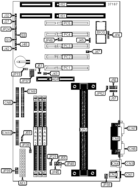
| I/O Options | 16-bit ISA slots (2), 32-bit PCI slots (5), AGP slot, ATX power connector, Floppy drive interface, IDE interfaces (2), IR connector, Parallel port, PS/2 keyboard port, PS/2 mouse port, Serial ports (2), USB interfaces (2), USB ports (2), Wake-on-LAN connector |
CONNECTIONS |
|||
Purpose |
Location |
Purpose |
Location |
| AGP slot | AGP | Green PC connector | J42 |
| ATX power connector | ATX | AGP fan power | J43 |
| PS/2 keyboard port | CN1 | Wake-on-LAN connector | J45 |
| PS/2 mouse port | CN2 | System fan power B | J47 |
| USB port 1 | CN3 | Green PC LED connector | J48 |
| USB port 2 | CN4 | Unidentified | J51 |
| Parallel port | CN5 | USB interface | J56 |
| Serial port 2 | CN6 | USB interface | J57 |
| Serial port 1 | CN7 | Unidentified | J59 |
| IDE interface 1 | CN8 | IR connector | JP4 |
| IDE interface 2 | CN9 | Speaker | JP24 |
| Floppy drive interface | CN10 | CPU fan power | JP29 |
| 16-bit ISA slots | IS1 - IS2 | SB-Link connector | JP46 |
| Power LED & keylock | J27 | 32-bit PCI slots | PC1 - PC5 |
| System fan power A | J28 | Power switch | S1 |
| Reset switch | J32 | IDE interface LED | S3 |
USER CONFIGURABLE SETTINGS |
|||
Function |
Label |
Position |
|
| » | 100MHz based processor normal bus speed | J55 | Open |
| 100MHz based processor overclocked to 133MHz | J55 | Closed | |
» |
CMOS memory normal operation | JP19 | Pins 1 & 2 closed |
| CMOS memory clear | JP19 | Pins 2 & 3 closed | |
| » | 66MHz based processor normal bus speed | JP45 | Open |
| 66MHz based processor overclocked to 100MHz | JP45 | Closed | |
| USB interfaces enabled | JP52 | Closed | |
| USB interfaces disabled | JP52 | Open | |
| Note: When overclocking, CPU setting must be auto configuration. | |||
DIMM CONFIGURATION |
|||
Size |
Bank 0 |
Bank 1 |
Bank 2 |
8MB |
(1) 1M x 64 |
None |
None |
16MB |
(1) 1M x 64 |
(1) 1M x 64 |
None |
16MB |
(1) 2M x 64 |
None |
None |
24MB |
(1) 1M x 64 |
(1) 1M x 64 |
(1) 1M x 64 |
32MB |
(1) 2M x 64 |
(1) 2M x 64 |
None |
32MB |
(1) 4M x 64 |
None |
None |
32MB |
(1) 2M x 64 |
(1) 1M x 64 |
(1) 1M x 64 |
48MB |
(1) 2M x 64 |
(1) 2M x 64 |
(1) 2M x 64 |
48MB |
(1) 4M x 64 |
(1) 1M x 64 |
(1) 1M x 64 |
64MB |
(1) 4M x 64 |
(1) 4M x 64 |
None |
64MB |
(1) 8M x 64 |
None |
None |
64MB |
(1) 4M x 64 |
(1) 2M x 64 |
(1) 2M x 64 |
80MB |
(1) 8M x 64 |
(1) 1M x 64 |
(1) 1M x 64 |
96MB |
(1) 4M x 64 |
(1) 4M x 64 |
(1) 4M x 64 |
96MB |
(1) 8M x 64 |
(1) 2M x 64 |
(1) 2M x 64 |
128MB |
(1) 8M x 64 |
(1) 8M x 64 |
None |
128MB |
(1) 16M x 64 |
None |
None |
128MB |
(1) 8M x 64 |
(1) 4M x 64 |
(1) 4M x 64 |
144MB |
(1) 16M x 64 |
(1) 1M x 64 |
(1) 1M x 64 |
160MB |
(1) 16M x 64 |
(1) 2M x 64 |
(1) 2M x 64 |
192MB |
(1) 8M x 64 |
(1) 8M x 64 |
(1) 8M x 64 |
192MB |
(1) 16M x 64 |
(1) 4M x 64 |
(1) 4M x 64 |
256MB |
(1) 16M x 64 |
(1) 16M x 64 |
None |
256MB |
(1) 32M x 64 |
None |
None |
256MB |
(1) 16M x 64 |
(1) 8M x 64 |
(1) 8M x 64 |
272MB |
(1) 32M x 64 |
(1) 1M x 64 |
(1) 1M x 64 |
288MB |
(1) 32M x 64 |
(1) 2M x 64 |
(1) 2M x 64 |
320MB |
(1) 32M x 64 |
(1) 4M x 64 |
(1) 4M x 64 |
384MB |
(1) 16M x 64 |
(1) 16M x 64 |
(1) 16M x 64 |
384MB |
(1) 32M x 64 |
(1) 8M x 64 |
(1) 8M x 64 |
512MB |
(1) 32M x 64 |
(1) 32M x 64 |
None |
512MB |
(1) 32M x 64 |
(1) 16M x 64 |
(1) 16M x 64 |
768MB |
(1) 32M x 64 |
(1) 32M x 64 |
(1) 32M x 64 |
| Note: Board supports SDRAM memory. | |||
CACHE CONFIGURATION |
| Note: 128KB cache is located on Celeron 300A and greater CPUs. 256/512 KB cache is located on the Pentium II and Pentium III CPUs. |
CPU SPEED SELECTION |
|||||
CPU Speed |
Clock Speed |
Multiplier |
JP37 |
JP39 |
|
| » | Auto | Auto | Auto | 2 & 3, 5 & 6, 8 & 9, 11 & 12,14 & 15 | N/A |
| 233MHz | 66MHz | 3.5x | 4 & 5, 10 & 11 | 5 & 6, 7 & 8 | |
| 266MHz | 66MHz | 4.0x | 7 & 8, 10 & 11, 13 & 14 | 5 & 6, 7 & 8 | |
300MHz |
66MHz |
4.5x |
7 & 8, 10 & 11 | 5 & 6, 7 & 8 | |
333MHz |
66MHz |
5.0x |
10 & 11, 13 & 14 | 5 & 6, 7 & 8 | |
350MHz |
100MHz |
3.5x |
4 & 5, 10 & 11 | 7 & 8 | |
| 366MHz | 66MHz |
5.5x |
10 & 11 | 5 & 6, 7 & 8 | |
| 400MHz | 66MHz | 6.0x | 4 & 5, 7 & 8, 13 & 14 | 5 & 6, 7 & 8 | |
| 400MHz | 100MHz | 4.0x | 7 & 8, 10 & 11, 13 & 14 | 7 & 8 | |
| 433MHz | 66MHz | 6.5x | 4 & 5, 7 & 8 | 5 & 6, 7 & 8 | |
| 450MHz | 100MHz | 4.5x | 7 & 8, 10 & 11 | 7 & 8 | |
| 500MHz | 100MHz | 5.0x | 10 & 11, 13 & 14 | 7 & 8 | |
Note: Designated pins should be in the closed position. |
|||||
POWER-ON BY KEYBOARD/MOUSE SELECTION |
||
Function |
JP38 |
|
| » | Power-on by keyboard enabled | Pins 1 & 3, 4 & 6 closed |
| Power-on by mouse enabled | Pins 2 & 4, 3 & 5 closed | |
| Power-on by keyboard/mouse enabled | Pins 3 & 5, 4 & 6 closed | |
| Power-on by keyboard/mouse disabled | Pins 1 & 3, 2 & 4 closed | |
CPU CORE VOLTAGE SELECTION |
|
Setting |
JP48 |
| Increased voltage by 0.15% | Pins 1 & 2 closed |
| Increase voltage by 0.5% | Pins 2 & 4 closed |
| Increase voltage by 1.5% | Pins 3 & 4 closed |
| Increased voltage by 7.8% | Pins 1 & 3 closed |