DOMEX TECHNOLOGY CORPORATION
SATURN (REV. 1A)
| Device Type | Mainboard |
| Processor | CX 6x86/CX6x86MX/CX MII/AM K5/AM K6/AM K6-2/IDT C6/RISE/Pentium/Pentium MMX |
| Processor Speed | 100/133/166/180/200/225/233/240/266/300/333/350/366/380/400/450MHz |
| Chip Set | VIA |
| Video Chip Set | Unidentified |
| Audio Chip Set | Unidentified |
| Maximum Onboard Memory | 256MB (EDO & SDRAM supported) |
| Maximum Video Memory | 8MB (SGRAM) |
| Maximum Audio Memory | Unidentified |
| Cache | 512KB |
| BIOS | Unidentified |
| Dimensions | 220mm x 213mm |
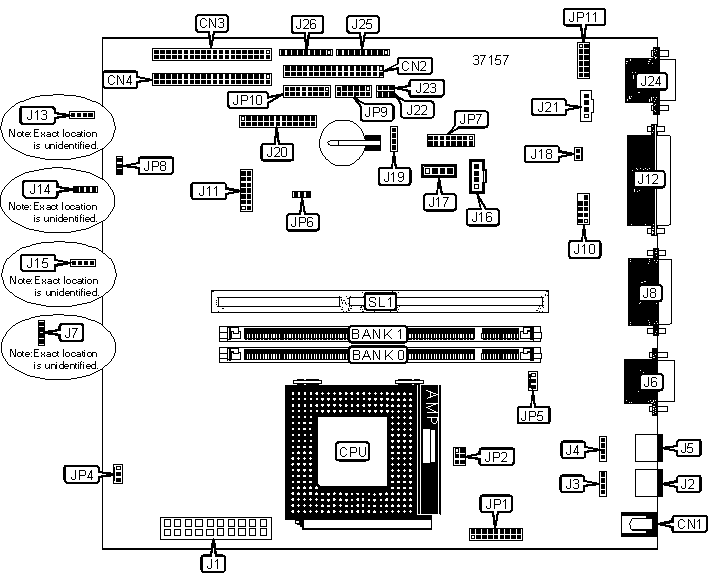
| I/O Options | ATX power connector, audio in - CD ROMs (2), composite out, daughterboard interfaces (2), floppy drive interface, game port, IDE interfaces (2), IR connectors (3), line in, line out, microphone in, parallel port, PS/2 keyboard port, PS/2 mouse port, riser slot, S-video out, serial interface, serial port, USB interface, VGA port, Wake-on-LAN connector, Wake-on-modem connector |
CONNECTIONS |
|||
Purpose |
Location |
Purpose |
Location |
| DC power connector | CN1 | Audio in - CD ROM (Sony) | J16 |
| Floppy drive interface | CN2 | Audio in - CD ROM (Panasonic) | J17 |
| IDE interface 1 | CN3 | Composite out connector | J18 |
| IDE interface 2 | CN4 | Capture module daughterboard interface | J20 |
| ATX power connector | J1 | S-video out interface | J21 |
| PS/2 keyboard port | J2 | Wake-on-LAN connector | J22 |
| IR mouse connector | J3 | Wake-on-modem connector | J23 |
| IR keyboard connector | J4 | VGA port | J24 |
| PS/2 mouse port | J5 | IR connector | J25/Pins 1 - 5 |
| Serial port 1 | J6 | Power switch | J25/Pins 6 & 7 |
| USB interface | J7 | IDE interface LED | J25/Pins 8 & 9 |
| Game port | J8 | Power LED | J26/Pins 1 - 3 |
| Serial interface | J10 | Speaker | J25/Pins 6 - 9 |
| Capture module daughterboard interface | J11 | System fan power | JP4 |
| Parallel port | J12 | CPU fan power | JP5 |
| Line in connector | J13 | TV out daughterboard connector | JP7 |
| Line out connector | J14 | TV out daughterboard connector | JP11 |
| Microphone in connector | J15 | Riser slot | SL1 |
USER CONFIGURABLE SETTINGS |
||
Function |
Label |
Position |
| CPU single voltage type | JP2 | Pins 1 & 3, 2 & 4 closed |
| CPU dual voltage type | JP2 | Pins 3 & 5, 4 & 6 closed |
| CPU SDRAM clock speed | JP6 | Pins 1 & 2 closed |
| AGP SDRAM clock speed | JP6 | Pins 2 & 3 closed |
Video format is NTSC |
JP8 |
Pins 2 & 3 closed |
| Video format PAL | JP8 |
Pins 1 & 2 closed |
DIMM CONFIGURATION |
||
Size |
Bank 0 |
Bank 1 |
8MB |
(1) 1M x 64 |
None |
16MB |
(1) 1M x 64 |
(1) 1M x 64 |
16MB |
(1) 2M x 64 |
None |
24MB |
(1) 2M x 64 |
(1) 1M x 64 |
32MB |
(1) 2M x 64 |
(1) 2M x 64 |
32MB |
(1) 4M x 64 |
None |
40MB |
(1) 4M x 64 |
(1) 1M x 64 |
48MB |
(1) 4M x 64 |
(1) 2M x 64 |
64MB |
(1) 4M x 64 |
(1) 4M x 64 |
64MB |
(1) 8M x 64 |
None |
72MB |
(1) 8M x 64 |
(1) 1M x 64 |
80MB |
(1) 8M x 64 |
(1) 2M x 64 |
96MB |
(1) 8M x 64 |
(1) 4M x 64 |
128MB |
(1) 8M x 64 |
(1) 8M x 64 |
128MB |
(1) 16M x 64 |
None |
136MB |
(1) 16M x 64 |
(1) 1M x 64 |
144MB |
(1) 16M x 64 |
(1) 2M x 64 |
160MB |
(1) 16M x 64 |
(1) 4M x 64 |
192MB |
(1) 16M x 64 |
(1) 8M x 64 |
256MB |
(1) 16M x 64 |
(1) 16M x 64 |
| Note: Board supports EDO & SDRAM memory. | ||
CMOS/BATTERY SELECTION |
|
Setting |
J19 |
| CMOS memory normal operation with internal battery | Pins 1 & 2 closed |
| CMOS memory normal operation with external battery | Pins 3 & 4 closed |
| CMOS memory clear | Open |
CPU SPEED SELECTION (CX 6X86MX) |
||||
CPU speed |
Clock speed |
Multiplier |
JP9 |
JP10 |
| 166MHz | 60MHz | 2.5x | Pins 1 & 2 | Pins 3 & 4 |
| 166MHz | 66MHz | 2.0x | Pins 3 & 4 | Pins 1 & 2 |
| 200MHz | 75MHz | 2.0x | Pins 5 & 6 | Pins 1 & 2 |
| 233MHx | 66MHz | 3.0x | Pins 3 & 4 | Pins 5 & 6 |
| 233MHz | 75MHz | 2.5x | Pins 5 & 6 | Pins 3 & 4 |
| 266MHz | 66MHz | 3.5x | Pins 3 & 4 | Pins 7 & 8 |
| 266MHz | 75MHz | 3.0x | Pins 5 & 6 | Pins 5 & 6 |
Note: Designated pins should be in the closed position. |
||||
CPU SPEED SELECTION (CX MII) |
||||
CPU speed |
Clock speed |
Multiplier |
JP9 |
JP10 |
| 300MHz | 66MHz | 3.5x | Pins 3 & 4 | Pins 7 & 8 |
| 300MHz | 75MHz | 3.0x | Pins 5 & 6 | Pins 5 & 6 |
| 333MHz | 83MHz | 3.0x | Pins 7 & 8 | Pins 5 & 6 |
| 350MHz | 83MHz | 3.0x | Pins 7 & 8 | Pins 5 & 6 |
| 366MHz | 100MHz | 2.5x | Pins 11 & 12 | Pins 3 & 4 |
Note: Designated pins should be in the closed position. |
||||
CPU SPEED SELECTION (AM K6) |
||||
CPU speed |
Clock speed |
Multiplier |
JP9 |
JP10 |
| 200MHz | 66MHz | 3.0x | Pins 3 & 4 | Pins 5 & 6 |
| 233MHz | 66MHz | 3.5x | Pins 3 & 4 | Pins 7 & 8 |
| 266MHz | 66MHz | 4.0x | Pins 3 & 4 | Pins 9 & 10 |
| 300MHz | 66MHz | 4.5x | Pins 3 & 4 | Pins 11 & 12 |
| 300MHz | 100MHz | 3.0x | Pins 11 & 12 | Pins 5 & 6 |
Note: Designated pins should be in the closed position. |
||||
CPU SPEED SELECTION (AM K6-2) |
||||
CPU speed |
Clock speed |
Multiplier |
JP9 |
JP10 |
| 233MHz | 66MHz | 3.5x | Pins 3 & 4 | Pins 7 & 8 |
| 266MHz | 66MHz | 4.0x | Pins 3 & 4 | Pins 9 & 10 |
| 300MHz | 66MHz | 4.5x | Pins 3 & 4 | Pins 11 & 12 |
| 300MHz | 100MHz | 3.0x | Pins 11 & 12 | Pins 5 & 6 |
| 333MHz | 66MHz | 5.0x | Pins 3 & 4 | Pins 13 & 14 |
| 333MHz | 95MHz | 3.5x | Pins 9 & 10 | Pins 7 & 8 |
| 350MHz | 100MHz | 3.5x | Pins 11 & 12 | Pins 7 & 8 |
| 380MHz | 95MHz | 4.0x | Pins 9 & 10 | Pins 9 & 10 |
| 400MHz | 100MHz | 4.0x | Pins 11 & 12 | Pins 9 & 10 |
| 450MHz | 100MHz | 4.5x | Pins 11 & 12 | Pins 11 & 12 |
Note: Designated pins should be in the closed position. |
||||
CPU SPEED SELECTION (ID C6) |
||||
CPU speed |
Clock speed |
Multiplier |
JP9 |
JP10 |
| 180MHz | 60MHz | 3.0x | Pins 1 & 2 | Pins 5 & 6 |
| 200MHz | 66MHz | 3.0x | Pins 3 & 4 | Pins 5 & 6 |
| 225MHz | 75MHz | 3.0x | Pins 5 & 6 | Pins 5 & 6 |
| 240MHz | 60MHz | 4.0x | Pins 1 & 2 | Pins 9 & 10 |
Note: Designated pins should be in the closed position. |
||||
CPU SPEED SELECTION (RISE) |
||||
CPU speed |
Clock speed |
Multiplier |
JP9 |
JP10 |
| 266MHz | 100MHz | 2.0x | Pins 11 & 12 | Pins 1 & 2 |
Note: Designated pins should be in the closed position. |
||||
CPU SPEED SELECTION (PENTIUM) |
||||
CPU speed |
Clock speed |
Multiplier |
JP9 |
JP10 |
| 100MHz | 66MHz | 1.5x | Pins 3 & 4 | Pins 7 & 8 |
| 133MHz | 66MHz | 2.0x | Pins 3 & 4 | Pins 1 & 2 |
| 166MHz | 66MHz | 2.5x | Pins 3 & 4 | Pins 3 & 4 |
| 200MHz | 66MHz | 3.0x | Pins 3 & 4 | Pins 5 & 6 |
Note: Designated pins should be in the closed position. |
||||
CPU SPEED SELECTION (PENTIUM MMX) |
||||
CPU speed |
Clock speed |
Multiplier |
JP9 |
JP10 |
| 166MHz | 66MHz | 2.5x | Pins 3 & 4 | Pins 3 & 4 |
| 200MHz | 66MHz | 3.0x | Pins 3 & 4 | Pins 5 & 6 |
| 233MHz | 66MHz | 3.5x | Pins 3 & 4 | Pins 7 & 8 |
Note: Designated pins should be in the closed position. |
||||
VOLTAGE SELECTION |
|
Voltage |
JP1 |
| 2.1V | Pins 1 & 2 closed |
| 2.2V | Pins 3 & 4 closed |
| 2.3V | Pins 5 & 6 closed |
| 2.4V | Pins 7 & 8 closed |
| 2.8V | Pins 9 & 10 closed |
| 2.9V | Pins 11 & 12 closed |
| 3.2V | Pins 13 & 14 closed |
| 3.3V | Pins 15 & 16 closed |
| 3.52V | Pins 17 & 18 closed |
| Device Type | Riser card |
| I/O Options | 32-bit PCI slot |
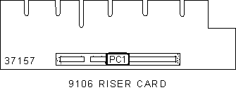
CONNECTIONS |
|
Purpose |
Location |
| 32-bit PCI slot | PC1 |
| Device Type | Riser card |
| I/O Options | 16-bit ISA slot, 32-bit PCI slots (2) |
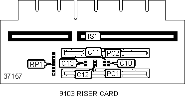
CONNECTIONS |
|||
Purpose |
Location |
Purpose |
Location |
| 16-bit ISA slot | IS1 | Unidentified | RP1 |
| 32-bit PCI slots | PC1 - PC2 | ||
USER CONFIGURABLE SETTINGS |
|||
Function |
Label |
Position |
|
| » | Factory configured - do not alter | C10 | Open |
| » | Factory configured - do not alter | C11 | Open |
| » | Factory configured - do not alter | C12 |
Open |
| » | Factory configured - do not alter | C13 |
Open |
| Device Type | Daughterboard |
| I/O Options | Composite in, S-video in, |
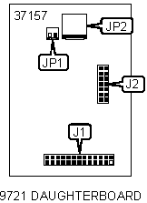
CONNECTIONS |
|||
Purpose |
Location |
Purpose |
Location |
| Mainboard connector | J1 | Composite video in connector | JP1 |
| Mainboard connector | J2 | S-video in connector | JP2 |
| Note: J1 connects to J20 on the mainboard. J2 connects to J11 on the mainboard. | |||
MISCELLANEOUS TECHNICAL NOTES |
| Diagram of 9720 Capture daughterboard not available. |