J-MARK COMPUTER CORPORATION
J-791BSR2
| Device Type | Mainboard |
| Processor | Pentium II/Celeron |
| Processor Speed | 233/266/300/333/350/366/400/433/450Mhz |
| Chip Set | VIA |
| Audio Chip Set | Unidentified |
| Maximum Onboard Memory | 512MB (EDO & SDRAM supported) |
| Cache | 0/128/256/512KB (located on the CPU) |
| BIOS | Award |
| Dimensions | 220mm x 230mm |
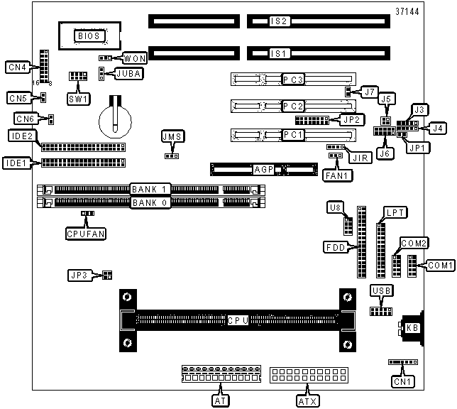
| I/O Options | 16-bit ISA slots (2), 32-bit PCI slots (3), AGP slot, AT keyboard port, AT power connector, ATX power connector, Audio in - CD-ROMs (2), Auxillary audio in, Floppy drive interface, Game interface, IDE interfaces (2), IR connector, Parallel port, PS/2 mouse interface, Serial ports (2), USB interface, Wake-on-LAN connector |
CONNECTIONS |
|||
| Purpose | Location |
Purpose | Location |
| AGP slot | AGP |
IDE interface 1 | IDE1 |
| AT power connector | AT |
IDE interface 2 | IDE2 |
| ATX power connector | ATX |
16-bit ISA slots | IS1 - IS2 |
| PS/2 mouse interface | CN1 | Audio in - CD-ROM 1 | J3 |
| Power LED & keylock | CN4/Pins 1 - 5 | Audio in - CD-ROM 2 | J4 |
| Turbo switch | CN4/Pins 6 - 8 | Digital audio in/out | J5 |
| Speaker | CN4/Pins 9 - 12 | Audio in | J6 |
| Reset switch | CN4/Pins 13 & 14 | IR connector | JIR |
| Turbo LED | CN4/Pins 15 & 16 | Unidentified | JP1 |
| IDE interface LED | CN5 | Game interface | JP2 |
| Power switch | CN6 | Unidentified | JP3 |
| Serial interface 1 | COM1 | AT keyboard port | KB |
| Serial interface 2 | COM2 | Parallel interface | LPT |
| CPU fan power | CPUFAN | 32-bit PCI slots | PC1 - PC3 |
| Fan power | FAN1 | USB interface | USB |
| Floppy drive interface | FDD | Wake-on-LAN connector | WON |
USER CONFIGURABLE SETTINGS |
|||
Function |
Label |
Position |
|
� |
On board sound enabled | J7 | Open |
| On board sound disabled | J7 | Closed | |
| PS/2 mouse IRQ select IRQ12 | JMS | Pins 1 & 2 closed |
|
| Other device IRQ select IRQ12 | JMS | Pins 2 & 3 closed |
|
� |
CMOS memory normal operation | JUBA |
Pins 1 & 2 closed |
| CMOS memory clear | JUBA |
Pins 2 & 3 closed |
|
DIMM CONFIGURATION |
||
Size |
Bank 0 |
Bank 1 |
16MB |
(1) 2M x 64 |
None |
32MB |
(1) 2M x 64 |
(1) 2M x 64 |
32MB |
(1) 4M x 64 |
None |
48MB |
(1) 4M x 64 |
(1) 2M x 64 |
64MB |
(1) 4M x 64 |
(1) 4M x 64 |
64MB |
(1) 8M x 64 |
None |
80MB |
(1) 8M x 64 |
(1) 2M x 64 |
96MB |
(1) 8M x 64 |
(1) 4M x 64 |
128MB |
(1) 8M x 64 |
(1) 8M x 64 |
128MB |
(1) 16M x 64 |
None |
144MB |
(1) 16M x 64 |
(1) 2M x 64 |
160MB |
(1) 16M x 64 |
(1) 4M x 64 |
192MB |
(1) 16M x 64 |
(1) 8M x 64 |
256MB |
(1) 16M x 64 |
(1) 16M x 64 |
256MB |
(1) 32M x 64 |
None |
272MB |
(1) 32M x 64 |
(1) 2M x 64 |
288MB |
(1) 32M x 64 |
(1) 4M x 64 |
320MB |
(1) 32M x 64 |
(1) 8M x 64 |
384MB |
(1) 32M x 64 |
(1) 16M x 64 |
512MB |
(1) 32M x 64 |
(1) 32M x 64 |
| Note: Board supports EDO & SDRAM memory. | ||
CACHE CONFIGURATION |
| Note: 256KB/512KB cache is located on the Pentium II CPUs. 128KB cache is located on the Celeron 300A and newer CPUs. |
CPU SPEED SELECTION (CELERON) |
||||
CPU speed |
Clock speed |
Multiplier |
U8 |
SW1 |
266MHz |
66MHz |
4x |
3 & 4, 5 & 6, 7 & 8 | 3 & 4, 5 & 6 |
300MHz |
66MHz |
4.5x |
3 & 4, 7 & 8 | 3 & 4, 5 & 6 |
333MHz |
66MHz |
5x |
5 & 6, 7 & 8 | 3 & 4, 5 & 6 |
| Note: Pins designated should be in the closed position. | ||||
CPU SPEED SELECTION (PENTIUM II) |
||||
CPU speed |
Clock speed |
Multiplier |
U8 |
SW1 |
233MHz |
66MHz |
3.5x |
1 & 2, 7 & 8 | 3 & 4, 5 & 6 |
266MHz |
66MHz |
4x |
3 & 4, 5 & 6, 7 & 8 | 3 & 4, 5 & 6 |
300MHz |
66MHz |
4.5x |
3 & 4, 7 & 8 | 3 & 4, 5 & 6 |
333MHz |
66MHz |
5x |
5 & 6, 7 & 8 | 3 & 4, 5 & 6 |
350MHz |
100MHz |
3.5x |
1 & 2, 7 & 8 | Open |
400MHz |
100MHz |
4x |
3 & 4, 5 & 6, 7 & 8 | Open |
450MHz |
100MHz |
4.5x |
3 & 4, 7 & 8 | Open |
Note: Pins designated should be in the closed position. |
||||