EMAC, INC.
PCM-4896
| Device Type | Single Board Computer |
| Processor | CX GXm |
| Processor Speed | 200/233/266/300MHz |
| Chip Set | Cyrix |
| Video Chip Set | Chips and Technology |
| Audio Chip Set | Cyrix |
| Maximum Onboard Memory | 128MB (SDRAM supported) |
| Maximum Video Memory | 2MB |
| Cache | 16KB (located on the CPU) |
| BIOS | Award |
| Dimensions | 203mm x 146mm |
| I/O Options | 32-bit PCI slot, ATX power connector, Audio in - CD-ROM, Solid-state flash disk socket, Ethernet 10BaseT connector, Flat panel connector, Floppy drive interface, IDE interface, IR connector, Parallel interface, PC/104 connector, PS/2 mouse/AT keyboard interface, Serial interfaces (4), Sound connector, USB interface, VGA connector |
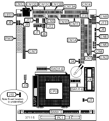
CONNECTIONS |
|||
| Purpose | Location |
Purpose | Location |
| 16-bit PC/104 connector | CN1 | Serial interface 2 | CN13B |
| 8-bit PC/104 connector | CN1A |
Serial interface 3 | CN13C |
| USB interface | CN2 |
Serial interface 4 | CN13D |
| IDE interface | CN4 |
Floppy drive interface | CN14 |
| Front panel connector | CN5 |
CPU fan power | J3 |
| IR connector | CN6 | Power switch | J5 |
| Flat panel connector | CN7 |
Audio in - CD-ROM | J7 |
| PS/2 mouse/AT keyboard interface | CN8 | Ethernet Rx LED connector | LED1/Pins 1 & 2 |
| VGA connector | CN9 | Ethernet Link LED connector | LED1/Pins 3 & 4 |
| Sound connector | CN10 |
Ethernet Tx LED connector | LED1/Pins 5 & 6 |
| Parallel interface | CN11 | 32-bit PCI slot | PC1 |
| 10BaseT Ethernet connector | CN12 |
ATX power connector | PW1 |
| Serial interface 1 | CN13A | Solid-state flash disk (DOC) socket | U4 |
| Note: Pin 1 location of LED1 is unidentified. | |||
USER CONFIGURABLE SETTINGS |
|||
Function |
Label |
Position |
|
| Internal buzzer selected | J1 |
Closed |
|
| External speaker slected | J1 |
Open |
|
» |
CMOS memory normal operation | J4 |
Pins 1 & 2 closed |
| CMOS memory clear | J4 |
Pins 2 & 3 closed |
|
| » | Audio output amplified | J6 |
Pins 3 & 5, 4 & 6 closed |
| Audio output not amplified | J6 | Pins 1 & 3, 2 & 4 closed |
|
| » | Flat panel connector (CN7) voltage select 3.3V | J8 |
Pins 2 & 3 closed |
| Flat panel connector (CN7) voltage select 5V | J8 |
Pins 1 & 2 closed |
|
| » | Flat panel clock signal select SHF | J9 | Pins 2 & 3 closed |
| Flat panel clock signal select ASHF | J9 | Pins 1 & 2 closed | |
» |
Factory configured - do not alter | J10 |
Pins 2 & 3 closed |
» |
Factory configured - do not alter | SW1/4 |
Unidentified |
» |
Factory configured - do not alter | SW2/2 | Unidentified |
» |
Factory configured - do not alter | SW2/3 | Unidentified |
» |
Factory configured - do not alter | SW2/4 | Unidentified |
» |
Factory configured - do not alter | SW2/5 | Unidentified |
» |
Factory configured - do not alter | SW2/6 | Unidentified |
| Note: Pin 1 locations of J4, J6, J8, J9, J10, SW1 & SW2 are unidentified. | |||
DIMM CONFIGURATION |
|
Size |
Bank 0 |
| 16MB | (1) 2M x 64 |
| 32MB | (1) 4M x 64 |
| 64MB | (1) 8M x 64 |
128MB |
(1) 16M x 64 |
| Note: Board supports SDRAM memory. | |
CPU SPEED SELECTION |
||||||
CPU speed |
Clock speed |
Multiplier |
SW1/1 |
SW1/2 | SW1/3 | SW2/1 |
| 200MHz | 33MHz | 6.0x | Off | On | Off | On |
| 233MHz | 33MHz | 7.0x | Off | Off | On | On |
| 266MHz | 30MHz | 9.0x | On | Off | On | Off |
| 300MHz | 30MHz | 10.0x | On | On | Off | Off |
Note: Pin 1 locations of SW1 & SW2 are unidentified. |
||||||
SERIAL INTERFACE 2 SELECTION |
|||
Setting |
J13 |
J14 |
|
| » | RS-232 |
Pins 1 & 2, 4 & 5, 7 & 8, 10 & 11 closed |
Pins 1 & 2 closed |
RS-422 |
Pins 2 & 3, 5 & 6, 8 & 9, 11 & 12 closed |
Pins 3 & 4 closed | |
RS-485 |
Pins 2 & 3, 5 & 6, 8 & 9, 11 & 12 closed |
Pins 5 & 6 closed | |
Note: Pin 1 locations of J13 & J14 are unidentified. All pins should be open unless designated as closed. |
|||
SERIAL INTERFACE 3 VOLTAGE SELECTION |
||||
Setting |
J12/Pins 1 & 2 |
J12/Pins 3 & 4 | J12/Pins 5 & 6 | |
| » | RI |
Open |
Open | Closed |
+5V |
Open |
Closed | Open | |
+12V |
Closed |
Open | Open | |
Note: Pin 1 location of J12 is unidentified. |
||||
SERIAL INTERFACE 4 VOLTAGE SELECTION |
||||
Setting |
J11/Pins 1 & 2 |
J11/Pins 3 & 4 | J11/Pins 5 & 6 | |
| » | RI |
Open |
Open | Closed |
+5V |
Open |
Closed | Open | |
+12V |
Closed |
Open | Open | |
Note: Pin 1 location of J11 is unidentified. |
||||
SOLID-STATE FLASH DISK (DOC) ADDRESS SELECTION |
||
Address |
SW1/5 |
SW1/6 |
Disable |
On |
On |
D400 |
Off |
Off |
| D800 | On | Off |
| DC00 | Off | On |
Note: Pin 1 location of SW1 is unidentified. |
||