AMPRO COMPUTERS, INC.
LITTLE BOARD/486SLC-IIA
| Device Type | Single Board Computer |
| Processor | CX486SLC/CX486SLC2 |
| Processor Speed | 25/50MHz |
| Chip Set | Unidentified |
| Maximum Onboard Memory | 16MB |
| Cache | Unidentified |
| BIOS | Award |
| Dimensions | 204mm x 146mm |
| I/O Options | Floppy drive interface, IDE interface, keyboard interface, parallel interface, PC/104 interfaces (2), SCSI interface, serial interfaces (2), utility interface |
| NPU Options | 80387SX |
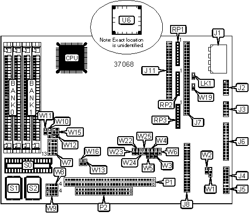
CONNECTIONS |
|||
| Purpose | Location |
Purpose | Location |
| Power connector | J1 | Floppy drive interface | J8 |
| Serial interface 2 | J2 | IDE interface | J11 |
| Serial interface 1 | J3 | Unidentified | LK1 |
| Utility interface | J4 | PC/104 interface (8-bit) | P1 |
| Keyboard interface | J5 | PC/104 interface (16-bit) | P2 |
| Parallel interface | J6 | Math coprocessor socket | U6 |
| SCSI interface | J7 | ||
| Note: The speed of the math coprocessor must be rated the same speed as the CPU. Adequate clearence is required for proper air flow. | |||
USER CONFIGURABLE SETTINGS |
|||
Function |
Label |
Position |
|
| » | Powerfail NMI disabled | W2 | Open |
| Powerfail NMI enabled | W2 | Closed | |
| » | Floppy interface enabled | W6 | Closed |
| Floppy interface disabled | W6 | Open | |
| » | Factory configured - do not alter | W13 | Open |
| » | Factory configured - do not alter | W15 | Pins 1 & 2, 3 & 4 closed |
| » | Factory configured - do not alter | W16 | Open |
| » | Factory configured - do not alter | W22 | Open |
SIMM CONFIGURATION |
||
Size |
Bank 0 |
Bank 1 |
512KB |
(2) 256K x 9 | None |
1MB |
(2) 256K x 9 |
(2) 256K x 9 |
2MB |
(2) 1M x 9 |
None |
4MB |
(2) 1M x 9 |
(2) 1M x 9 |
8MB |
(2) 4M x 9 |
None |
16MB |
(2) 4M x 9 |
(2) 4M x 9 |
| Note: Modules of 70ns or lower are supported. | ||
EPROM CONFIGURATION (S0) |
||
EPROM |
Pins | W7 |
| 8K (27C64) | 28 | 8 & 9, 14 & 15 |
| 8K (EEPROM) (28C64) | 28 | 8 & 9, 14 & 15 |
| 16K (27C128) | 28 | 8 & 9, 14 & 15 |
| 32K (27C256) | 28 | 9 & 12, 14 & 15 |
| 64K (27C512) | 28 | 9 & 12, 10 & 11, 14 & 15 |
| 128K (27C010) | 32 | 2 & 5, 7 & 8, 9 & 12, 10 & 11 |
| 256K (27C020) | 32 | 2 & 5, 7 & 8, 9 & 12, 10 & 11, 13 & 14 |
| 512K (27C040) | 32 | 2 & 5, 4 & 7, 9 & 12, 10 & 11, 13 & 14 |
| 1MB (27C080) | 32 | 4 & 7, 5 & 6, 9 & 12, 10 & 11, 13 & 14 |
Note: Designated pins should be in the closed position. |
||
FLASH EPROM CONFIGURATION (S0) |
||
Flash EPROM |
Pins | W7 |
| 32K 5V (29C256) | 28 | 8 & 11, 9 & 12, 14 & 15 |
| 32K 5V (28C256) | 28 | 8 & 9, 11 & 12, 14 & 15 |
| 64K 5V (29F512) | 32 | 4 & 5, 7 & 8, 9 & 12, 10 & 11, 13 & 14 |
| 128K 5V (29F010) | 32 | 4 & 5, 7 & 8, 9 & 12, 10 & 11, 13 & 14 |
| 256K 5V (29F020) | 32 | 4 & 5, 7 & 8, 9 & 12, 10 & 11, 13 & 14 |
| 512K 5V (29F040) | 32 | 4 & 5, 7 & 8, 9 & 12, 10 & 11, 13 & 14 |
| 32K 12V (28F256) | 32 | 2 & 5, 7 & 8, 9 & 12, 10 & 11, 13 & 14 |
| 64K 12V (28F512) | 32 | 2 & 5, 7 & 8, 9 & 12, 10 & 11, 13 & 14 |
| 128K 12V (28F010) | 32 | 2 & 5, 7 & 8, 9 & 12, 10 & 11, 13 & 14 |
| 256K 12V (28F020) | 32 | 2 & 5, 7 & 8, 9 & 12, 10 & 11, 13 & 14 |
Note: Designated pins should be in the closed position. |
||
SRAM CONFIGURATION (S0) |
||
SRAM |
Pins | W7 |
| 32K (43256) | 28 | 7 & 10, 8 & 9, 11 & 12, 14 & 15 |
| 128 K (628128) | 32 | 7 & 10, 8 & 9, 11 & 12, 14 & 15 |
| 512K (628512) | 32 | 4 & 5, 7 & 10, 8 & 9, 11 & 12, 13 & 14 |
Note: Designated pins should be in the closed position. |
||
NOVRAM CONFIGURATION (S0) |
||
Chip Type |
Pins | W7 |
| 32K (Dallas DS1235Y) | 32 | 7 & 10, 8 & 9, 11 & 12, 14 & 15 |
| 32K (Benchmarq BQ4013Y) | 32 | 7 & 10, 8 & 9, 11 & 12, 14 & 15 |
| 512K (Dallas DS1650Y) | 32 | 4 & 5, 7 & 10, 8 & 9, 11 & 12, 13 & 14 |
| 512K (Benchmarq BQ4015Y) | 32 | 4 & 5, 7 & 10, 8 & 9, 11 & 12, 13 & 14 |
Note: Designated pins should be in the closed position. |
||
EPROM CONFIGURATION (S1) |
|
EPROM |
W8 |
| 128K | Pins 3 & 4, 6 & 7 closed |
| 256K | Pins 3 & 4, 6 & 7 closed |
FLASH EPROM CONFIGURATION (S1) |
|
Flash EPROM |
W8 |
| 128K | Pins 3 & 4, 5 & 6 closed |
| 256K | Pins 3 & 4, 5 & 6 closed |
EPROM CONFIGURATION (S2) |
|
EPROM |
W9 |
| 128K | Pins 3 & 4, 6 & 7 closed |
| 256K | Pins 3 & 4, 6 & 7 closed |
FLASH EPROM CONFIGURATION (S2) |
|
Flash EPROM |
W9 |
| 128K | Pins 3 & 4, 5 & 6 closed |
| 256K | Pins 3 & 4, 5 & 6 closed |
WATCHDOG TIMER CONFIGURATION |
||
Setting |
W1 | |
| » | Watchdog timer is disabled | Open |
| Alarm causes I/O channel check | Pins 1 & 2 closed | |
| Alarm causes reset | Pins 2 & 3 closed | |
DMA CHANNEL SELECTION |
||
Channel |
W3 | W4 |
1 |
Pins 1 & 2 closed | Pins 1 & 2 closed |
3 |
Pins 2 & 3 closed | Pins 2 & 3 closed |
PARALLEL PORT INTERRUPT SELECTION |
||
IRQ |
W5 | |
| » | IRQ7 |
Pins 1 & 2 closed |
IRQ5 |
Pins 2 & 3 closed | |
| None | Open | |
BATTERY BACKUP SELECTION |
|||
Setting |
W10 | W11 | |
| » | Battery backup to S0 disabled |
Pins 2 & 3 closed | Off |
Battery backup to S0 enabled |
Pins 1 & 2 closed | On | |
Note: The battery backup enabled setting makes the SRAM in S0 non-volatile. If an EPROM or Flash EPROM is used in S0, use the battery backup disabled setting which sets the power to S0 as Vcc. |
|||
SCSI INTERFACE SELECTION |
||||
SCSI Interface |
W12 | W23 | W24 | W25 |
Enabled |
Closed | Closed | Closed | Closed |
Disabled |
Open | Open | Open | Open |
Note: SCSI termination should be disabled as well. |
||||
SCSI HOST TERMINATION SELECTION |
|||
Setting |
RP1 | RP2 | RP3 |
Termination enabled |
Closed | Closed | Closed |
Termination disabled |
Open | Open | Open |
TERMINATION POWER SELECTION |
||
Setting |
W19 | |
| » | Termination power disabled |
Open |
TERMPWR supplied by SCSI interface pin 26 |
Closed | |
UTILITY CONNECTOR (J4) PIN CONFIGURATION |
||
Pin |
Signal Name |
Function |
1 |
Speaker |
Audio signal |
2 |
Speaker |
Ground |
3 |
Ground |
To one side of Reset button |
4 |
Reset |
To other side of Reset button |
5 |
LED Cathode |
Ground return |
6 |
LED anode |
Current source (+5v through 330 ohms) |
7 |
Ground |
Ground return |
8 |
+12V power |
Connected to J9 pin B9 |
9 |
-5V power |
Connected to J9 pin B5 |
10 |
-12V power |
Connected to J9 pin B7 |
11 |
Ground |
Ground return |
12 |
POWERGOOD |
Power supply status |