NMC INTERNATIONAL
NMC 6BCDSX+ (SMP)
| Device Type | Mainboard |
| Processor | Pentium II |
| Processor Speed | 200/233/266/300/333/350/366/400/450MHz |
| Chip Set | Intel 440BX |
| Maximum Onboard Memory | 1024MB (EDO & SDRAM supported) |
| Cache | 256/512KB (located on the Pentium II CPU) |
| BIOS | Award |
| Dimensions | Unidentified |
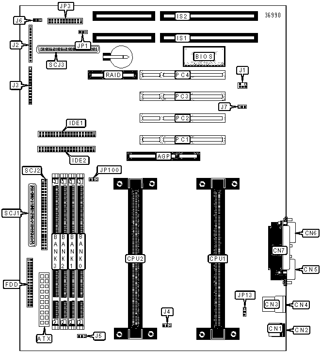
| I/O Options | 16-bit ISA slots (2), 32-bit PCI slots (4), floppy drive interface, IDE interfaces (2), SCSI connector, SCSI Wide connector, Ultra2 SCSI connector, parallel port, IR connector, PS/2 mouse port, PS/2 keyboard port, serial ports (2), USB ports (2), ATX power connector, AGP slot, SB-Link connector, Wake-on-LAN connector |
CONNECTIONS |
|||
| Purpose | Location |
Purpose | Location |
| AGP slot | AGP |
Speaker | J2/Pins 4 - 7 |
| ATX power connector | ATX |
Power LED & keylock | J2/Pins 9 - 13 |
| PS/2 mouse port | CN1 | IR connector | J3/Pins 1 - 5 |
| PS/2 keyboard port | CN2 | IDE interface LED | J3/Pins 7 & 8 |
| USB port 1 | CN3 | Turbo LED | J3/Pins 9 & 10 |
| USB port 2 | CN4 | Soft off power connector | J3/Pins 12 & 13 |
| Serial port 1 | CN5 | CPU fan power 1 | J4 |
| Serial port 2 | CN6 | CPU fan power 2 | J5 |
| Parallel port | CN7 | Chassis fan power | J6 |
| Floppy drive interface | FDD | Wake-on-LAN connector | J7 |
| IDE interface 1 | IDE1 | 32-bit PCI slots | PC1 - PC4 |
| IDE interface 2 | IDE2 | RAID connector | RAID |
| 16-bit ISA slots | IS1 - IS3 | SCSI Wide connector | SCJ1 |
| SB-Link connector | J1 | SCSI connector | SCJ2 |
| Reset switch | J2/Pins 1 & 2 | Ultra2 SCSI connector | SCJ3 |
USER CONFIGURABLE SETTINGS |
|||
Function |
Label |
Position |
|
» |
CMOS memory normal operation | JP1 |
Pins 1 & 2 closed |
| CMOS memory clear | JP1 |
Pins 2 & 3 closed |
|
| » | Factory configued - do not alter | JP3 | Pins 13 & 14 reserved |
| » | Factory configued - do not alter | JP3 | Pins 15 & 16 reserved |
| » | Factory configued - do not alter | JP3 | Pins 17 & 18 reserved |
| » | Factory configued - do not alter | JP3 | Pins 19 & 20 reserved |
| » | Factory configued - do not alter | JP3 | Pins 21 & 22 reserved |
| » | Factory configued - do not alter | JP3 | Pins 22 & 24 reserved |
| » | Power-on Keyboard disabled | JP13 | Pins 2 & 3 closed |
| Power-on Keyboard enabled | JP13 | Pins 1 & 2 closed | |
| » | Auto bus clock select | JP100 | Pins 1 & 2 closed |
| 100MHz bus clock select | JP100 | Pins 2 & 3 closed | |
| DIMM CONFIGURATION | ||||
Size |
Bank 0 |
Bank 1 |
Bank 2 |
Bank 3 |
8MB |
(1) 1M x 64 |
None |
None |
None |
16MB |
(1) 1M x 64 |
(1) 1M x 64 |
None |
None |
16MB |
(1) 2M x 64 |
None |
None |
None |
24MB |
(1) 1M x 64 |
(1) 1M x 64 |
(1) 1M x 64 |
None |
32MB |
(1) 1M x 64 |
(1) 1M x 64 |
(1) 1M x 64 |
(1) 1M x 64 |
32MB |
(1) 2M x 64 |
(1) 2M x 64 |
None |
None |
32MB |
(1) 4M x 64 |
None |
None |
None |
48MB |
(1) 2M x 64 |
(1) 2M x 64 |
(1) 2M x 64 |
None |
64MB |
(1) 2M x 64 |
(1) 2M x 64 |
(1) 2M x 64 |
(1) 2M x 64 |
64MB |
(1) 4M x 64 |
(1) 4M x 64 |
None |
None |
64MB |
(1) 8M x 64 |
None |
None |
None |
80MB |
(1) 4M x 64 |
(1) 4M x 64 |
(1) 1M x 64 |
(1) 1M x 64 |
96MB |
(1) 4M x 64 |
(1) 4M x 64 |
(1) 4M x 64 |
None |
96MB |
(1) 4M x 64 |
(1) 4M x 64 |
(1) 2M x 64 |
(1) 2M x 64 |
128MB |
(1) 4M x 64 |
(1) 4M x 64 |
(1) 4M x 64 |
(1) 4M x 64 |
128MB |
(1) 8M x 64 |
(1) 8M x 64 |
None |
None |
128MB |
(1) 16M x 64 |
None |
None |
None |
144MB |
(1) 8M x 64 |
(1) 8M x 64 |
(1) 1M x 64 |
(1) 1M x 64 |
160MB |
(1) 8M x 64 |
(1) 8M x 64 |
(1) 2M x 64 |
(1) 2M x 64 |
192MB |
(1) 8M x 64 |
(1) 8M x 64 |
(1) 8M x 64 |
None |
192MB |
(1) 8M x 64 |
(1) 8M x 64 |
(1) 4M x 64 |
(1) 4M x 64 |
256MB |
(1) 8M x 64 |
(1) 8M x 64 |
(1) 8M x 64 |
(1) 8M x 64 |
256MB |
(1) 16M x 64 |
(1) 16M x 64 |
None |
None |
256MB |
(1) 32M x 64 |
None |
None |
None |
272MB |
(1) 16M x 64 |
(1) 16M x 64 |
(1) 1M x 64 |
(1) 1M x 64 |
288MB |
(1) 16M x 64 |
(1) 16M x 64 |
(1) 2M x 64 |
(1) 2M x 64 |
320MB |
(1) 16M x 64 |
(1) 16M x 64 |
(1) 4M x 64 |
(1) 4M x 64 |
384MB |
(1) 16M x 64 |
(1) 16M x 64 |
(1) 16M x 64 |
None |
384MB |
(1) 16M x 64 |
(1) 16M x 64 |
(1) 8M x 64 |
(1) 8M x 64 |
512MB |
(1) 16M x 64 |
(1) 16M x 64 |
(1) 16M x 64 |
(1) 16M x 64 |
| *512MB | (1) 32M x 64 |
(1) 32M x 64 |
None |
None |
| *528MB | (1) 32M x 64 |
(1) 32M x 64 |
(1) 1M x 64 |
(1) 1M x 64 |
| *544MB | (1) 32M x 64 |
(1) 32M x 64 |
(1) 2M x 64 |
(1) 2M x 64 |
| *576MB | (1) 32M x 64 |
(1) 32M x 64 |
(1) 4M x 64 |
(1) 4M x 64 |
| *640MB | (1) 32M x 64 |
(1) 32M x 64 |
(1) 8M x 64 |
(1) 8M x 64 |
| *768MB | (1) 32M x 64 |
(1) 32M x 64 |
(1) 32M x 64 |
None |
| *768MB | (1) 32M x 64 |
(1) 32M x 64 |
(1) 16M x 64 |
(1) 16M x 64 |
| *1024MB | (1) 32M x 64 |
(1) 32M x 64 |
(1) 32M x 64 |
(1) 32M x 64 |
| Note: Board
supports EDO & SDRAM memory. Maximum SDRAM is 512MB. Maximum EDO is 1024MB. *: Memory configurations require EDO memory. |
||||
CACHE CONFIGURATION |
| Note: 256KB/512KB cache is located on the Pentium II CPUs. |
CPU SPEED SELECTION |
|||
CPU Speed |
Clock Speed | JP3 | |
|
200MHz | 66MHz | Pins 1 & 2 closed |
| 233MHz | 66MHz | Pins 3 & 4 closed | |
| » | 266MHz | 66MHz | Pins 5 & 6 closed |
| 300MHz | 66MHz | Pins 7 & 8 closed | |
| 300MHz | 100MHz | Pins 1 & 2 closed | |
| 333MHz | 66MHz | Pins 9 & 10 closed | |
| 350MHz | 100MHz | Pins 3 & 4 closed | |
| 366MHz | 66MHz | Pins 11 & 12 closed | |
| 400MHz | 100MHz | Pins 5 & 6 closed | |
| 450MHz | 100MHz | Pins 7 & 8 closed | |
| 500MHz | 100MHz | Pins 9 & 10 closed | |
| 550MHz | 100MHz | Pins 11 & 12 closed | |