AST RESEARCH, INC.
PREMIUM GS 6233 (503453-101)
| Device Type | Mainboard |
| Processor | Pentium II |
| Processor Speed | 233/266/300/333/366MHz |
| Chip Set | Intel 440LX |
| Video Chip Set | Cirrus Logic |
| Maximum Onboard Memory | 256/512MB (SDRAM supported) |
| Maximum Video Memory | 1MB |
| Cache | 512KB (located on the Pentium II CPU) |
| BIOS | Unidentified |
| Dimensions | 330mm x 305mm |
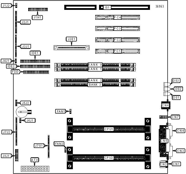
| I/O Options | 16-bit ISA slot, 32-bit PCI slots (4), Ethernet 10BaseT connector, floppy drive interface, IDE interfaces (2), Wide SCSI interface, parallel port, PS/2 mouse port, PS/2 keyboard port, serial port, serial interface, VGA port, ATX power connector |
CONNECTIONS |
|||
| Purpose | Location |
Purpose | Location |
| ATX power connector | ATX |
IDE interface 2 | IDE2 |
| PS/2 mouse port | CN1 | 16-bit ISA slot | IS1 |
| PS/2 keyboard port | CN2 | SMM connector | J1H1 |
| Serial port | CN3 | System fan power 1 | J1J2 |
| VGA port | CN4 | Wide SCSI interface | J3E1 |
| Parallel port | CN5 | System fan power 2 | J4J1 |
| Ethernet 10BaseT connector | CN6 | IDE interface LED | J5J2 |
| Serial interface | CN7 | Local I2C connector | J6J1 |
| Heat sink fan 1 | FAN1 | AT front panel connector | J7J2 |
| Heat sink fan 2 | FAN2 | Front panel connector | J8J1 |
| Floppy drive interface | FDD | 32-bit PCI slots | PC1 - PC4 |
| IDE interface 1 | IDE1 | ||
USER CONFIGURABLE SETTINGS |
|||
Function |
Label |
Position |
|
» |
CMOS memory normal operation | J2J1 |
Pins 1 & 2 closed |
| CMOS memory clear | J2J1 |
Pins 2 & 3 closed |
|
| Password enabled | J2J1 | Pins 5 & 6 closed |
|
| Password disabled | J2J1 | Pins 6 & 7 closed |
|
| Normal boot enabled | J2J1 | Pins 9 & 10 closed | |
| Recovery boot enabled, BIOS loaded from disk | J2J1 |
Pins 10 & 11 closed |
|
| BIOS write protection enabled | J2J1 |
Pins 13 & 14 closed |
|
| BIOS write protection disabled | J2J1 |
Pins 14 & 15 closed |
|
| CPU speed configuration disabled | J3J1 |
Pins 1 & 2 closed |
|
| CPU speed configuration enabled | J3J1 |
Pins 2 & 3 closed |
|
| FRB timer enabled | J3J1 |
Pins 5 & 6 closed |
|
| FRB timer disabled | J3J1 |
Pins 6 & 7 closed | |
| Chassis intrusion detect enabled | J3J1 |
Pins 9 & 10 closed |
|
| Chassis intrusion detect disabled | J3J1 |
Pins 10 & 11 closed |
|
| Minimum in-order queue host bus | J3J1 |
Pins 13 & 14 closed |
|
| Maximum in-order queue host bus | J3J1 |
Pins 14 & 15 closed |
|
| DIMM CONFIGURATION | ||||
Size |
Bank 0 |
Bank 1 |
Bank 2 |
Bank 3 |
8MB |
(1) 1M x 64 |
None |
None |
None |
16MB |
(1) 1M x 64 |
(1) 1M x 64 |
None |
None |
16MB |
(1) 2M x 64 |
None |
None |
None |
24MB |
(1) 1M x 64 |
(1) 1M x 64 |
(1) 1M x 64 |
None |
32MB |
(1) 1M x 64 |
(1) 1M x 64 |
(1) 1M x 64 |
(1) 1M x 64 |
32MB |
(1) 2M x 64 |
(1) 2M x 64 |
None |
None |
32MB |
(1) 4M x 64 |
None |
None |
None |
48MB |
(1) 2M x 64 |
(1) 2M x 64 |
(1) 2M x 64 |
None |
64MB |
(1) 2M x 64 |
(1) 2M x 64 |
(1) 2M x 64 |
(1) 2M x 64 |
64MB |
(1) 4M x 64 |
(1) 4M x 64 |
None |
None |
64MB |
(1) 8M x 64 |
None |
None |
None |
80MB |
(1) 4M x 64 |
(1) 4M x 64 |
(1) 1M x 64 |
(1) 1M x 64 |
96MB |
(1) 4M x 64 |
(1) 4M x 64 |
(1) 4M x 64 |
None |
96MB |
(1) 4M x 64 |
(1) 4M x 64 |
(1) 2M x 64 |
(1) 2M x 64 |
128MB |
(1) 4M x 64 |
(1) 4M x 64 |
(1) 4M x 64 |
(1) 4M x 64 |
128MB |
(1) 8M x 64 |
(1) 8M x 64 |
None |
None |
128MB |
(1) 16M x 64 |
None |
None |
None |
144MB |
(1) 8M x 64 |
(1) 8M x 64 |
(1) 1M x 64 |
(1) 1M x 64 |
160MB |
(1) 8M x 64 |
(1) 8M x 64 |
(1) 2M x 64 |
(1) 2M x 64 |
192MB |
(1) 8M x 64 |
(1) 8M x 64 |
(1) 8M x 64 |
None |
192MB |
(1) 8M x 64 |
(1) 8M x 64 |
(1) 4M x 64 |
(1) 4M x 64 |
256MB |
(1) 8M x 64 |
(1) 8M x 64 |
(1) 8M x 64 |
(1) 8M x 64 |
256MB |
(1) 16M x 64 |
(1) 16M x 64 |
None |
None |
256MB |
(1) 32M x 64 |
None |
None |
None |
272MB |
(1) 16M x 64 |
(1) 16M x 64 |
(1) 1M x 64 |
(1) 1M x 64 |
288MB |
(1) 16M x 64 |
(1) 16M x 64 |
(1) 2M x 64 |
(1) 2M x 64 |
320MB |
(1) 16M x 64 |
(1) 16M x 64 |
(1) 4M x 64 |
(1) 4M x 64 |
384MB |
(1) 16M x 64 |
(1) 16M x 64 |
(1) 16M x 64 |
None |
384MB |
(1) 16M x 64 |
(1) 16M x 64 |
(1) 8M x 64 |
(1) 8M x 64 |
512MB |
(1) 16M x 64 |
(1) 16M x 64 |
(1) 16M x 64 |
(1) 16M x 64 |
| Note: Board supports SDRAM memory. | ||||
CACHE CONFIGURATION |
| Note: 256KB/512KB cache is located on the Pentium II CPUs. |
CPU SPEED SELECTION |
||||
Speed |
J7G1/Pins 1 & 2 | J7G1/Pins 2 & 3 | J7G1/Pins 5 & 6 | J7G1/Pins 6 & 7 |
233MHz |
Open | Closed | Closed | Open |
| 266MHz | Closed | Open | Open | Closed |
| 300MHz | Closed | Open | Open | Closed |
| 333MHz | Open | Open | Open | Closed |
| 366MHz | Open | Open | Open | Closed |
CPU SPEED SELECTION |
||||
Speed |
J7G1/Pins 9 & 10 | J7G1/Pins 10 & 11 | J7G1/Pins 13 & 14 | J7G1/Pins 14 & 15 |
233MHz |
Open | Closed | Closed | Open |
| 266MHz | Closed | Open | Closed | Open |
| 300MHz | Open | Closed | Closed | Open |
| 333MHz | Closed | Open | Closed | Open |
| 366MHz | Open | Closed | Closed | Open |
DIAGNOSTIC LED(S) |
||
LED |
Status |
Condition |
| DS1 | On | Network controller at 100Mbps transfer speed operation |
| DS1 | Off | Network controller at 10Mbps transfer speed operation |
| DS2 | On | Link to LAN; network controller & hub receiving power; or cable connection good |
| DS2 | Off | No Link to LAN; network controller & hub not receiving power; or cable connection bad |
| DS3 | On (Blinking) | Network controller sending or receiving data |
| DS3 | Off | Network controller not sending or receiving data |