ACER, INC.
P2/370A-V (VER. 1.1)
| Device Type | Mainboard |
| Processor | Celeron/Pentium II/Pentium III |
| Processor Speed | 266/300/333/350/366/400/433/450/466/500MHz |
| Chip Set | VIA |
| Audio Chip Set | ESS |
| Maximum Onboard Memory | 768MB (EDO & SDRAM supported) |
| Maximum Audio Memory | Unidentified |
| Cache | 0/128/256/512KB (located on the CPU) |
| BIOS | Award |
| Dimensions | 305mm x 170mm |
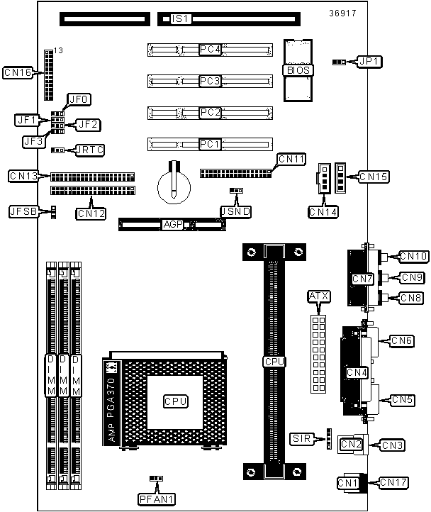
| I/O Options | 16-bit ISA slot, 32-bit PCI slots (4), floppy drive interface, game port, green PC connector, IDE interfaces (2), parallel port, PS/2 mouse port, PS/2 keyboard port, serial ports (2), IR connector, USB ports (2), ATX power connector, AGP slot, line in, line out, microphone in, audio in - CD-ROMs (2), Wake-on-LAN connector |
CONNECTIONS |
|||
| Purpose | Location |
Purpose | Location |
| AGP slot | AGP |
IDE interface 2 | CN13 |
| ATX power connector | ATX |
Audio in - CD-ROM (Sony) | CN14 |
| PS/2 mouse port | CN1 | Audio in - CD-ROM (Mitsumi) | CN15 |
| USB port 1 | CN2 | Green PC LED | CN16/Pins 1 & 2 |
| USB port 2 | CN3 | Reset switch | CN16/Pins 3 & 4 |
| Parallel port | CN4 | IDE interface LED | CN16/Pins 6 & 7 |
| Serial port 1 | CN5 | Power switch | CN16/Pins 9 & 10 |
| Serial port 2 | CN6 | Green PC connector | CN16/Pins 11 & 12 |
| Game port | CN7 | Power LED & keylock | CN16/Pins 14-18 |
| Line out | CN8 | Speaker | CN16/Pins 20-23 |
| Line in | CN9 | Wake-on-LAN connector | JP1 |
| Microphone in | CN10 | 32-bit PCI slots | PC1 - PC4 |
| Floppy drive interface | CN11 | CPU fan power | PFAN1 |
| IDE interface 1 | CN12 | IR connector | SIR |
USER CONFIGURABLE SETTINGS |
|||
Function |
Label |
Position |
|
» |
CMOS memory normal operation | JRTC | Pins 2 & 3 closed |
| CMOS memory clear | JRTC | Pins 1 & 2 closed | |
| » | On-board audio enabled | JSND | Pins 1 & 2 closed |
|
On-board audio disabled | JSND | Pins 2 & 3 closed |
| External clock speed set to auto-detect | JFSB | Open | |
| Note: External clock speed may also be set to 100MHz and 66MHz. See tables below. | |||
DIMM CONFIGURATION |
|||
Size |
Bank 0 |
Bank 1 |
Bank 2 |
8MB |
(1) 1M x 64 |
None |
None |
16MB |
(1) 1M x 64 |
(1) 1M x 64 |
None |
16MB |
(1) 2M x 64 |
None |
None |
24MB |
(1) 1M x 64 |
(1) 1M x 64 |
(1) 1M x 64 |
32MB |
(1) 2M x 64 |
(1) 2M x 64 |
None |
32MB |
(1) 4M x 64 |
None |
None |
32MB |
(1) 2M x 64 |
(1) 1M x 64 |
(1) 1M x 64 |
48MB |
(1) 2M x 64 |
(1) 2M x 64 |
(1) 2M x 64 |
48MB |
(1) 4M x 64 |
(1) 1M x 64 |
(1) 1M x 64 |
64MB |
(1) 4M x 64 |
(1) 4M x 64 |
None |
64MB |
(1) 8M x 64 |
None |
None |
64MB |
(1) 4M x 64 |
(1) 2M x 64 |
(1) 2M x 64 |
80MB |
(1) 8M x 64 |
(1) 1M x 64 |
(1) 1M x 64 |
96MB |
(1) 4M x 64 |
(1) 4M x 64 |
(1) 4M x 64 |
96MB |
(1) 8M x 64 |
(1) 2M x 64 |
(1) 2M x 64 |
128MB |
(1) 8M x 64 |
(1) 8M x 64 |
None |
128MB |
(1) 16M x 64 |
None |
None |
128MB |
(1) 8M x 64 |
(1) 4M x 64 |
(1) 4M x 64 |
144MB |
(1) 16M x 64 |
(1) 1M x 64 |
(1) 1M x 64 |
160MB |
(1) 16M x 64 |
(1) 2M x 64 |
(1) 2M x 64 |
192MB |
(1) 8M x 64 |
(1) 8M x 64 |
(1) 8M x 64 |
192MB |
(1) 16M x 64 |
(1) 4M x 64 |
(1) 4M x 64 |
256MB |
(1) 16M x 64 |
(1) 16M x 64 |
None |
256MB |
(1) 32M x 64 |
None |
None |
256MB |
(1) 16M x 64 |
(1) 8M x 64 |
(1) 8M x 64 |
272MB |
(1) 32M x 64 |
(1) 1M x 64 |
(1) 1M x 64 |
288MB |
(1) 32M x 64 |
(1) 2M x 64 |
(1) 2M x 64 |
320MB |
(1) 32M x 64 |
(1) 4M x 64 |
(1) 4M x 64 |
384MB |
(1) 16M x 64 |
(1) 16M x 64 |
(1) 16M x 64 |
384MB |
(1) 32M x 64 |
(1) 8M x 64 |
(1) 8M x 64 |
512MB |
(1) 32M x 64 |
(1) 32M x 64 |
None |
512MB |
(1) 32M x 64 |
(1) 16M x 64 |
(1) 16M x 64 |
768MB |
(1) 32M x 64 |
(1) 32M x 64 |
(1) 32M x 64 |
| Note: Board supports EDO & SDRAM memory. | |||
CACHE CONFIGURATION |
| Note: 512 KB cache is located on the Pentium III CPUs. 256KB/512KB cache is located on the Pentium II CPUs. 128KB cache is located on the Celeron 300A and greater CPUs. |
CPU SPEED SELECTION (CELERON) |
|||||||
CPU speed |
Clock speed |
Multiplier |
JF0 |
JF1 |
JF2 |
JF3 | JFSB |
266MHz |
66MHz |
4x |
2 & 3 | 1 & 2 | 1 & 2 | 1 & 2 | 2 & 3 |
300MHz |
66MHz |
4.5x |
2 & 3 | 1 & 2 | 2 & 3 | 1 & 2 | 2 & 3 |
333MHz |
66MHz |
5x |
2 & 3 | 2 & 3 | 1 & 2 | 1 & 2 | 2 & 3 |
366MHz |
66MHz |
5.5x |
2 & 3 | 2 & 3 | 2 & 3 | 1 & 2 | 2 & 3 |
| 400MHz | 66MHz | 6x | 1 & 2 | 1 & 2 | 1 & 2 | 2 & 3 | 2 & 3 |
| 433MHz | 66MHz | 6.5x | 1 & 2 | 1 & 2 | 2 & 3 | 2 & 3 | 2 & 3 |
| 466MHz | 66MHz | 7x | 1 & 2 | 2 & 3 | 2 & 3 | 2 & 3 | 2 & 3 |
| 500MHz | 66MHz | 7.5x | 1 & 2 | 2 & 3 | 2 & 3 | 2 & 3 | 2 & 3 |
Note: Designated pins should be in the closed position. |
|||||||
CPU SPEED SELECTION (PENTIUM II) |
|||||||
CPU speed |
Clock speed |
Multiplier |
JF0 |
JF1 |
JF2 |
JF3 | JFSB |
| 233MHz | 66MHz | 3.5x | 1 & 2 | 2 & 3 | 2 & 3 | 1 & 2 | 2 & 3 |
266MHz |
66MHz |
4x |
2 & 3 | 1 & 2 | 1 & 2 | 1 & 2 | 2 & 3 |
300MHz |
66MHz |
4.5x |
2 & 3 | 1 & 2 | 2 & 3 | 1 & 2 | 2 & 3 |
333MHz |
66MHz |
5x |
2 & 3 | 2 & 3 | 1 & 2 | 1 & 2 | 2 & 3 |
350MHz |
100MHz |
3.5 |
1 & 2 | 2 & 3 | 2 & 3 | 1 & 2 | 1 & 2 |
| 400MHz | 100MHz | 4x | 2 & 3 | 1 & 2 | 1 & 2 | 1 & 2 | 1 & 2 |
| 450MHz | 100MHz | 4.5x | 2 & 3 | 1 & 2 | 2 & 3 | 1 & 2 | 1 & 2 |
Note: Designated pins should be in the closed position. |
|||||||
CPU SPEED SELECTION (PENTIUM II) |
|||||||
CPU speed |
Clock speed |
Multiplier |
JF0 |
JF1 |
JF2 |
JF3 | JFSB |
| 450MHz | 100MHz | 4.5x | 2 & 3 | 1 & 2 | 2 & 3 | 1 & 2 | 1 & 2 |
| 500MHz | 100MHz | 5x | 2 & 3 | 2 & 3 | 1 & 2 | 1 & 2 | 1 & 2 |
Note: Designated pins should be in the closed position. |
|||||||