SOYO COMPUTER CO., LTD.
SY-71WA-F
| Device Type | Mainboard |
| Processor | Celeron |
| Processor Speed | 300A/333/366/400/433/466/500MHz |
| Chip Set | Intel 810 |
| Video Chip Set | Intel |
| Audio Chip Set | Unidentified |
| Maximum Onboard Memory | 512MB (SDRAM supported) |
| Maximum Video Memory | 4MB |
| Maximum Audio Memory | Unidentified |
| Cache | 128KB (located on the Celeron CPU) |
| BIOS | Unidentified |
| Dimensions | Unidentified |
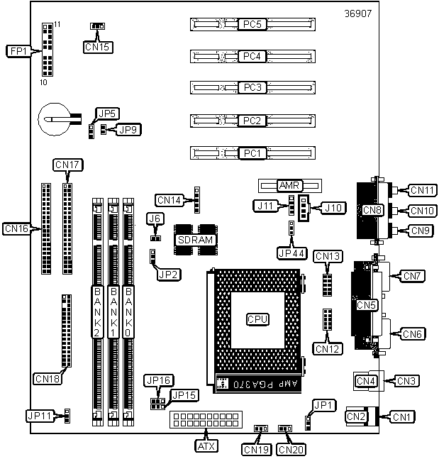
| I/O Options | 32-bit PCI slots (5), AMR slot, ATX power connector, audio in - CD-ROMs (2), digital flat panel connector, floppy drive interface, game/MIDI port, IDE interfaces (2), IR connector, line in, line out, microphone in, parallel port, PS/2 keyboard port, PS/2 mouse port, serial interfaces (2), USB ports (2), VGA port, Wake-on-LAN connector |
CONNECTIONS |
|||
Purpose |
Location |
Purpose |
Location |
| Audio modem riser slot | AMR | System fan power | CN15 |
| ATX power connector | ATX | IDE interface 1 | CN16 |
| PS/2 keyboard port | CN1 | IDE interface 2 | CN17 |
| PS/2 mouse port | CN2 | Floppy drive interface | CN18 |
| USB port 1 | CN3 | Power supply fan power | CN19 |
| USB port 2 | CN4 | CPU fan power | CN20 |
| Parallel port | CN5 | Reset switch | FP1/Pins 1 & 2 |
| VGA port | CN6 | Power switch | FP1/Pins 4 & 5 |
| Digital flat panel connector | CN7 | ACPI LED | FP1/Pins 7 & 8 |
| Game/MIDI port | CN8 | IDE interface LED | FP1/Pins 9 & 10 |
| Line out | CN9 | Power LED & keylock | FP1/Pins 11 - 15 |
| Line in | CN10 | Speaker | FP1/Pins 17 - 20 |
| Microphone in | CN11 | Audio in - CD-ROM | J10 |
| Serial interface 1 | CN12 | Audio in - CD-ROM | J11 |
| Serial interface 2 | CN13 | Wake-on-LAN connector | JP44 |
| IR connector | CN14 | 32-bit PCI slots | PC1 - PC5 |
USER CONFIGURABLE SETTINGS |
|||
Function |
Label |
Position |
|
| Power-on by keyboard is enabled | JP1 | Pins 1 & 2 closed | |
| Power-on by keyboard is disabled | JP1 | Pins 2 & 3 closed | |
» |
CMOS memory normal operation | JP5 | Pins 1 & 2 closed |
| CMOS memory clear | JP5 | Pins 2 & 3 closed | |
| FWH boot block is write protected | JP9 | Open | |
| FWH boot block is not write protected | JP9 | Closed | |
| Power-on by hot key of USB keyboard is enabled | JP11 | Pins 1 & 2 closed | |
| Power-on by hot key of USB keyboard is disabled | JP11 | Pins 2 & 3 closed | |
DIMM CONFIGURATION |
|||
Size |
Bank 0 |
Bank 1 |
Bank 2 |
8MB |
(1) 1M x 64 |
None |
None |
16MB |
(1) 1M x 64 |
(1) 1M x 64 |
None |
16MB |
(1) 2M x 64 |
None |
None |
24MB |
(1) 1M x 64 |
(1) 1M x 64 |
(1) 1M x 64 |
32MB |
(1) 2M x 64 |
(1) 2M x 64 |
None |
32MB |
(1) 4M x 64 |
None |
None |
32MB |
(1) 2M x 64 |
(1) 1M x 64 |
(1) 1M x 64 |
48MB |
(1) 2M x 64 |
(1) 2M x 64 |
(1) 2M x 64 |
48MB |
(1) 4M x 64 |
(1) 1M x 64 |
(1) 1M x 64 |
64MB |
(1) 4M x 64 |
(1) 4M x 64 |
None |
64MB |
(1) 8M x 64 |
None |
None |
64MB |
(1) 4M x 64 |
(1) 2M x 64 |
(1) 2M x 64 |
80MB |
(1) 8M x 64 |
(1) 1M x 64 |
(1) 1M x 64 |
96MB |
(1) 4M x 64 |
(1) 4M x 64 |
(1) 4M x 64 |
96MB |
(1) 8M x 64 |
(1) 2M x 64 |
(1) 2M x 64 |
128MB |
(1) 8M x 64 |
(1) 8M x 64 |
None |
128MB |
(1) 16M x 64 |
None |
None |
128MB |
(1) 8M x 64 |
(1) 4M x 64 |
(1) 4M x 64 |
144MB |
(1) 16M x 64 |
(1) 1M x 64 |
(1) 1M x 64 |
160MB |
(1) 16M x 64 |
(1) 2M x 64 |
(1) 2M x 64 |
192MB |
(1) 8M x 64 |
(1) 8M x 64 |
(1) 8M x 64 |
192MB |
(1) 16M x 64 |
(1) 4M x 64 |
(1) 4M x 64 |
256MB |
(1) 16M x 64 |
(1) 16M x 64 |
None |
256MB |
(1) 32M x 64 |
None |
None |
256MB |
(1) 16M x 64 |
(1) 8M x 64 |
(1) 8M x 64 |
272MB |
(1) 32M x 64 |
(1) 1M x 64 |
(1) 1M x 64 |
288MB |
(1) 32M x 64 |
(1) 2M x 64 |
(1) 2M x 64 |
320MB |
(1) 32M x 64 |
(1) 4M x 64 |
(1) 4M x 64 |
384MB |
(1) 16M x 64 |
(1) 16M x 64 |
(1) 16M x 64 |
384MB |
(1) 32M x 64 |
(1) 8M x 64 |
(1) 8M x 64 |
512MB |
(1) 32M x 64 |
(1) 32M x 64 |
None |
512MB |
(1) 32M x 64 |
(1) 16M x 64 |
(1) 16M x 64 |
| Note: Board supports SDRAM
memory. Note: PC100 compliant DIMM modules must be used. |
|||
CACHE CONFIGURATION |
| Note: 128KB cache is located on Celeron 300A and greater CPUs. |
CPU FSB SPEED SELECTION |
||
FSB Speed |
J6 |
JP2 |
Auto |
Closed |
Open |
66MHz |
Open |
Pins 1 & 2 closed |
100MHz |
Open |
Pins 2 & 3 closed |
CPU CORE VOLTAGE SELECTION |
||
Setting |
JP15 |
JP16 |
Default Vcore |
Pins 1 & 2 closed |
Open |
2.5% higher |
Pins 2 & 3 closed |
Open |
5.0% higher |
Open |
Pins 1 & 2 closed |
7.5% higher |
Open |
Pins 2 & 3 closed |