FAMOUS TECHNOLOGY CO., LTD.
MP-6VIP (REV. 1.00)
| Device Type | Mainboard |
| Processor | Celeron/Pentium II |
| Processor Speed | 233/266/300/333/350/400/450/500MHz |
| Chip Set | VIA |
| Maximum Onboard Memory | 1GB (SDRAM supported) |
| Cache | 0/128/256/512KB (located on the CPU) |
| BIOS | Award |
| Dimensions | 305mm x 170mm |
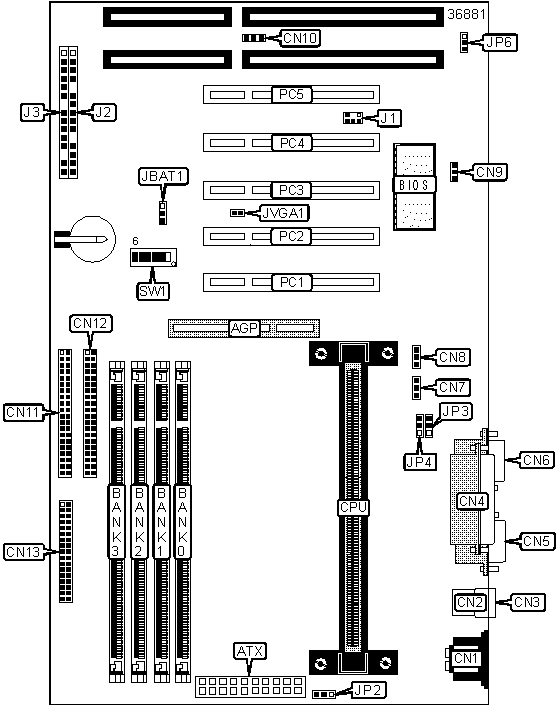
| I/O Options | 32-bit PCI slots (5), AGP slot, ATX power connector, floppy drive interface, green PC connector, IDE interfaces (2), IR connector, parallel port, PS/2 mouse port, SB-Link connector, serial ports (2), USB ports (2), Wake-on-LAN connector |
CONNECTIONS |
|||
Purpose |
Location |
Purpose |
Location |
| AGP slot | AGP | IDE interface 2 | CN12 |
| ATX power connector | ATX | Floppy drive interface | CN13 |
| PS/2 mouse port | CN1 | SB-Link connector | J1 |
| USB port 1 | CN2 | IDE interface LED | J2/Pins 1 - 4 |
| USB port 2 | CN3 | IR connector | J2/Pins 6 - 10 |
| Parallel port | CN4 | Power switch | J2/Pins 12 & 13 |
| Serial port 1 | CN5 | Green PC switch | J2/Pins 14 & 15 |
| Serial port 2 | CN6 | Speaker | J3/Pins 1 - 4 |
| System fan power | CN7 | Reset switch | J3/Pins 5 & 6 |
| CPU fan power | CN8 | Power LED & keylock | J3/Pins 8 - 12 |
| Wake-on-LAN connector | CN9 | Green LED | J3/Pins 14 & 15 |
| Chassis fan power | CN10 | 32-bit PCI slots | PC1-PC5 |
| IDE interface 1 | CN11 | ||
USER CONFIGURABLE SETTINGS |
|||
Function |
Label |
Position |
|
» |
CMOS memory normal operation | JBAT1 | Pins 1 & 2 closed |
| CMOS memory clear | JBAT1 | Pins 2 & 3 closed | |
| » | Power on by keyboard disabled | JP2 | Pins 1 & 2 closed |
| Power on by keyboard enabled | JP2 | Pins 2 & 3 closed | |
| » | Use power switch on the mainboard | JP6 | Pins 1 & 2 closed |
| Use ATX power supply to control on/off switch | JP6 | Pins 2 & 3 closed | |
| » | VGA card normal | JVGA1 | Closed |
| VGA card special | JVGA1 | Open | |
DIMM CONFIGURATION |
||||
Size |
Bank 0 |
Bank 1 |
Bank 2 |
Bank 3 |
8MB |
(1) 1M x 64 |
None |
None |
None |
16MB |
(1) 1M x 64 |
(1) 1M x 64 |
None |
None |
16MB |
(1) 2M x 64 |
None |
None |
None |
24MB |
(1) 1M x 64 |
(1) 1M x 64 |
(1) 1M x 64 |
None |
32MB |
(1) 1M x 64 |
(1) 1M x 64 |
(1) 1M x 64 |
(1) 1M x 64 |
32MB |
(1) 2M x 64 |
(1) 2M x 64 |
None |
None |
32MB |
(1) 4M x 64 |
None |
None |
None |
48MB |
(1) 2M x 64 |
(1) 2M x 64 |
(1) 2M x 64 |
None |
64MB |
(1) 2M x 64 |
(1) 2M x 64 |
(1) 2M x 64 |
(1) 2M x 64 |
64MB |
(1) 4M x 64 |
(1) 4M x 64 |
None |
None |
64MB |
(1) 8M x 64 |
None |
None |
None |
80MB |
(1) 4M x 64 |
(1) 4M x 64 |
(1) 1M x 64 |
(1) 1M x 64 |
96MB |
(1) 4M x 64 |
(1) 4M x 64 |
(1) 4M x 64 |
None |
96MB |
(1) 4M x 64 |
(1) 4M x 64 |
(1) 2M x 64 |
(1) 2M x 64 |
128MB |
(1) 4M x 64 |
(1) 4M x 64 |
(1) 4M x 64 |
(1) 4M x 64 |
128MB |
(1) 8M x 64 |
(1) 8M x 64 |
None |
None |
128MB |
(1) 16M x 64 |
None |
None |
None |
144MB |
(1) 8M x 64 |
(1) 8M x 64 |
(1) 1M x 64 |
(1) 1M x 64 |
160MB |
(1) 8M x 64 |
(1) 8M x 64 |
(1) 2M x 64 |
(1) 2M x 64 |
192MB |
(1) 8M x 64 |
(1) 8M x 64 |
(1) 8M x 64 |
None |
192MB |
(1) 8M x 64 |
(1) 8M x 64 |
(1) 4M x 64 |
(1) 4M x 64 |
256MB |
(1) 8M x 64 |
(1) 8M x 64 |
(1) 8M x 64 |
(1) 8M x 64 |
256MB |
(1) 16M x 64 |
(1) 16M x 64 |
None |
None |
256MB |
(1) 32M x 64 |
None |
None |
None |
272MB |
(1) 16M x 64 |
(1) 16M x 64 |
(1) 1M x 64 |
(1) 1M x 64 |
288MB |
(1) 16M x 64 |
(1) 16M x 64 |
(1) 2M x 64 |
(1) 2M x 64 |
320MB |
(1) 16M x 64 |
(1) 16M x 64 |
(1) 4M x 64 |
(1) 4M x 64 |
384MB |
(1) 16M x 64 |
(1) 16M x 64 |
(1) 16M x 64 |
None |
384MB |
(1) 16M x 64 |
(1) 16M x 64 |
(1) 8M x 64 |
(1) 8M x 64 |
512MB |
(1) 16M x 64 |
(1) 16M x 64 |
(1) 16M x 64 |
(1) 16M x 64 |
512MB |
(1) 32M x 64 |
(1) 32M x 64 |
None |
None |
528MB |
(1) 32M x 64 |
(1) 32M x 64 |
(1) 1M x 64 |
(1) 1M x 64 |
544MB |
(1) 32M x 64 |
(1) 32M x 64 |
(1) 2M x 64 |
(1) 2M x 64 |
576MB |
(1) 32M x 64 |
(1) 32M x 64 |
(1) 4M x 64 |
(1) 4M x 64 |
640MB |
(1) 32M x 64 |
(1) 32M x 64 |
(1) 8M x 64 |
(1) 8M x 64 |
768MB |
(1) 32M x 64 |
(1) 32M x 64 |
(1) 32M x 64 |
None |
768MB |
(1) 32M x 64 |
(1) 32M x 64 |
(1) 16M x 64 |
(1) 16M x 64 |
1024MB |
(1) 32M x 64 |
(1) 32M x 64 |
(1) 32M x 64 |
(1) 32M x 64 |
| Note: Board supports SDRAM memory. | ||||
CACHE CONFIGURATION |
| Note: 256/512KB cache is located on Pentium II CPUs. 128KB cache is located on Celeron 300A and greater CPUs. |
USB SELECTION |
|||
Setting |
JP3 |
JP4 |
|
| » | USB ports are redirected to USB connector | Pins 1 & 2 closed | Pins 1 & 2 closed |
| USB1 is redirected to AGP port | Pins 2 & 3 closed | Pins 2 & 3 closed | |
CPU SPEED SELECTION |
||||||||
CPU speed |
Clock speed |
Multiplier |
SW1/1 | SW1/2 | SW1/3 | SW1/4 | SW1/5 | SW1/6 |
| 233MHz | 66MHz | 3.5x | On | Off | Off | On | On | Off |
| 266MHz | 66MHz | 4.0x | Off | On | On | On | On | Off |
| 300MHz | 66MHz | 4.5x | Off | On | Off | On | On | Off |
| 333MHz | 66MHz | 5.0x | Off | Off | On | On | On | Off |
| 350MHz | 100MHz | 3.5x | On | Off | Off | On | Off | Off |
| 400MHz | 100MHz | 4.0x | Off | On | On | On | Off | Off |
| 450MHz | 100MHz | 4.5x | Off | On | Off | On | Off | Off |
| 500MHz | 100MHz | 5.0x | Off | Off | On | On | Off | Off |
Note: To use the auto-detect (default) bus clock setting, SW1/5 is off, and SW1/6 is on. |
||||||||