FIRST INTERNATIONAL COMPUTER, INC.
KA-6100
| Device Type | Mainboard |
| Processor | Pentium II/Celeron |
| Processor Speed | 233/266/300/333/350/366/400/450MHz |
| Chip Set | VIA |
| Audio Chip Set | Yamaha |
| Maximum Onboard Memory | 384MB (SDRAM supported) |
| Maximum Audio Memory | Unidentified |
| Cache | 0/128/256/512KB (located on the CPU) |
| BIOS | Unidentified |
| Dimensions | 218mm x 230mm |
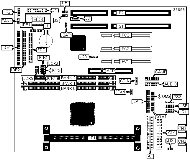
| I/O Options | 32-bit PCI slots (3), 16-bit ISA slots (2), floppy drive interface, game interface, IDE interfaces (2), parallel interface, PS/2 keyboard port, PS/2 mouse port, PS/2 mouse interface, serial interfaces (2), IR connector (2), USB interface, ATX power connector, AGP slot, AT power connector, audio in - CD-ROM, Audio connector, Front panel connector |
CONNECTIONS |
|||
| Purpose | Location |
Purpose | Location |
| AGP slot | AGP | Game interface | GAME |
| AT power connector | AT | IDE interface 1 | IDE1 |
| ATX power connector | ATX | IDE interface 2 | IDE2 |
| Audio connector | AUDIO | IR connector 1 | IR1 |
| Audio in - CD-ROM | CDIN | IR connector 2 | IR2 |
| CPU fan power | CFAN | 16-bit ISA slots | IS1 - IS2 |
| PS/2 keyboard port | CN2 | Unidentified | J3 |
| PS/2 mouse port | CN3 | Front panel connector | J4 |
| Serial port 1 | COM1 | Parallel interface | LPT |
| Serial port 2 | COM2 | 32-bit PCI slots | PC1 - PC3 |
| Chassis fan power | FAN1 | PS/2 mouse interface | PS2 |
| Floppy drive interface | FDD | USB interface | USB |
USER CONFIGURABLE SETTINGS |
|||
Function |
Label |
Position |
|
» |
CMOS memory normal operation | JBAT1 | Pins 1 & 2 closed |
| CMOS memory clear | JBAT1 | Pins 2 & 3 closed | |
| 2MB Flash ROM selected | JPE1 | Pins 1 & 2 closed | |
|
1MB Flach ROM selected | JPE1 |
Pins 2 & 3 closed |
| ATX power selected | J13 |
Pins 1 & 2 closed |
|
| AT power selected | J13 |
Pins 2 & 3 closed |
|
| Flash BIOS voltage select 12v | J15 | Pins 2 & 3 closed |
|
| Flash BIOS voltage select 5v | J15 | Pins 1 & 2 closed | |
| Password normal operation | J20 | Open | |
| Password clear | J20 | Closed | |
DIMM CONFIGURATION |
|||
Size |
Bank 0 |
Bank 1 |
Bank 2 |
8MB |
(1) 1M x 64 |
None |
None |
16MB |
(1) 1M x 64 |
(1) 1M x 64 |
None |
16MB |
(1) 2M x 64 |
None |
None |
24MB |
(1) 1M x 64 |
(1) 1M x 64 |
(1) 1M x 64 |
32MB |
(1) 2M x 64 |
(1) 2M x 64 |
None |
32MB |
(1) 4M x 64 |
None |
None |
32MB |
(1) 2M x 64 |
(1) 1M x 64 |
(1) 1M x 64 |
48MB |
(1) 2M x 64 |
(1) 2M x 64 |
(1) 2M x 64 |
48MB |
(1) 4M x 64 |
(1) 1M x 64 |
(1) 1M x 64 |
64MB |
(1) 4M x 64 |
(1) 4M x 64 |
None |
64MB |
(1) 8M x 64 |
None |
None |
64MB |
(1) 4M x 64 |
(1) 2M x 64 |
(1) 2M x 64 |
80MB |
(1) 8M x 64 |
(1) 1M x 64 |
(1) 1M x 64 |
96MB |
(1) 4M x 64 |
(1) 4M x 64 |
(1) 4M x 64 |
96MB |
(1) 8M x 64 |
(1) 2M x 64 |
(1) 2M x 64 |
128MB |
(1) 8M x 64 |
(1) 8M x 64 |
None |
128MB |
(1) 16M x 64 |
None |
None |
128MB |
(1) 8M x 64 |
(1) 4M x 64 |
(1) 4M x 64 |
144MB |
(1) 16M x 64 |
(1) 1M x 64 |
(1) 1M x 64 |
160MB |
(1) 16M x 64 |
(1) 2M x 64 |
(1) 2M x 64 |
192MB |
(1) 8M x 64 |
(1) 8M x 64 |
(1) 8M x 64 |
192MB |
(1) 16M x 64 |
(1) 4M x 64 |
(1) 4M x 64 |
256MB |
(1) 16M x 64 |
(1) 16M x 64 |
None |
256MB |
(1) 32M x 64 |
None |
None |
256MB |
(1) 16M x 64 |
(1) 8M x 64 |
(1) 8M x 64 |
272MB |
(1) 32M x 64 |
(1) 1M x 64 |
(1) 1M x 64 |
288MB |
(1) 32M x 64 |
(1) 2M x 64 |
(1) 2M x 64 |
320MB |
(1) 32M x 64 |
(1) 4M x 64 |
(1) 4M x 64 |
384MB |
(1) 16M x 64 |
(1) 16M x 64 |
(1) 16M x 64 |
384MB |
(1) 32M x 64 |
(1) 8M x 64 |
(1) 8M x 64 |
512MB |
(1) 32M x 64 |
(1) 32M x 64 |
None |
512MB |
(1) 32M x 64 |
(1) 16M x 64 |
(1) 16M x 64 |
768MB |
(1) 32M x 64 |
(1) 32M x 64 |
(1) 32M x 64 |
| Note: Board supports EDO & SDRAM memory. | |||
CACHE CONFIGURATION |
| Note: 256KB/512KB cache is located on the Pentium II CPUs. 128KB cache is located on the Celeron 300A and greater CPUs. |
CPU SPEED SELECTION (PENTIUM) |
|||||
CPU Clock speed |
SDRAM Clock Speed |
JCK1 |
JCK2 |
JCK3 |
JCK4 |
103MHz |
66MHz |
2 & 3 |
1 & 2 | 1 & 2 | 1 & 2 |
103MHz |
103MHz |
2 & 3 |
1 & 2 | 1 & 2 | 2 & 3 |
100MHz |
66MHz |
2 & 3 |
1 & 2 | 2 & 3 | 1 & 2 |
100MHz |
100MHz |
2 & 3 |
1 & 2 | 2 & 3 | 2 & 3 |
| 75MHz | 75MHz | 1 & 2 | 2 & 3 | 2 & 3 | N/A |
| 66MHz | 66MHz | 2 & 3 | 2 & 3 | 2 & 3 | N/A |
Note: Pins designated should be in the closed position |
|||||
CPU MULTIPLIER SELECTION |
||||
Multiplier |
JCK5/Pins 1 & 2 | JCK5/Pins 3 & 4 | JCK5/Pins 5 & 6 | JCK5/Pins 7 & 8 |
3x |
Closed | Open | Closed | Closed |
3.5x |
Closed | Open | Open | Closed |
4x |
Open | Closed | Closed | Closed |
4.5x |
Open | Closed | Open | Closed |
| 5x | Open | Open | Closed | Closed |
| 5.5x | Open | Open | Open | Closed |