PINE TECHNOLOGY
PT-7502-2A01
| Device Type | Mainboard |
| Processor | CX 6X86/AM K5/Pentium/Pentium MMX |
| Processor Speed | 75/90/100/120/133/150/166/180/200MHz |
| Chip Set | Intel 430VX |
| Maximum Onboard Memory | 128MB (EDO & SDRAM supported) |
| Cache | 256/512KB |
| BIOS | Award |
| Dimensions | Unidentified |
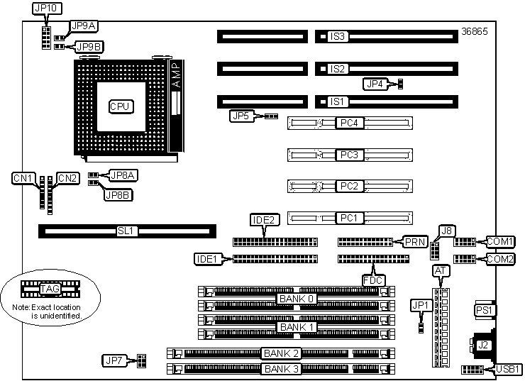
| I/O Options | 32-bit PCI slots (4), 16-bit ISA slots (2), floppy drive interface, green PC connector, IDE interfaces (2), AT Keyboard port, parallel interface, PS/2 mouse port, PS/2 mouse interface, serial interfaces (2), cache slot, USB interface, AT power connector |
CONNECTIONS |
|||
| Purpose | Location |
Purpose | Location |
| AT power connector | AT | IDE interface 1 | IDE1 |
| Reset switch | CN1/Pins 1 & 2 | IDE interface 2 | IDE2 |
| IDE interface LED | CN1/Pins 3 & 4 | 16-bit ISA slots | IS1 - IS3 |
| LED connector | CN1/Pins 5 & 6 | AT keyboard port | J2 |
| Power switch | CN1/Pins 7 & 8 | PS/2 mouse interface | J8 |
| Power LED & keylock | CN2/Pins 1 - 5 | 32-bit PCI slots | PC1 - PC4 |
| Speaker | CN2/Pins 6 - 9 | Parallel interface | PRN |
| Serial interface 1 | COM1 | PS/2 mouse port | PS1 |
| Serial interface 2 | COM2 | USB interface | USB1 |
| Floppy drive interface | FDC | Cache slot | SL1 |
USER CONFIGURABLE SETTINGS |
|||
Function |
Label |
Position |
|
» |
CMOS memory normal operation | JP1 | Open |
| CMOS memory clear | JP1 | Closed | |
» |
AT bus clock = PCI clock/4 | JP4 |
Pins 1 & 2 closed |
| AT bus clock = PCI clock/3 | JP4 |
Pins 2 & 3 closed |
|
| Flash BIOS voltage select 12v | JP5 |
Pins 1 & 2 closed |
|
| Flash BIOS voltage select 5v | JP5 |
Pins 2 & 3 closed |
|
| » | Factory configured - do not alter | JP7A | Unidentified |
| » | Factory configured - do not alter | JP7B | Unidentified |
SIMM CONFIGURATION |
||
Size |
Bank 0 |
Bank 1 |
8MB |
(2) 1M x 36 |
None |
16MB |
(2) 2M x 36 |
None |
16MB |
(2) 1M x 36 |
(2) 1M x 36 |
24MB |
(2) 2M x 36 |
(2) 1M x 36 |
32MB |
(2) 4M x 36 |
None |
32MB |
(2) 2M x 36 |
(2) 2M x 36 |
40MB |
(2) 4M x 36 |
(2) 1M x 36 |
48MB |
(2) 4M x 36 |
(2) 2M x 36 |
64MB |
(2) 8M x 36 |
None |
64MB |
(2) 4M x 36 |
(2) 4M x 36 |
72MB |
(2) 8M x 36 |
(2) 1M x 36 |
80MB |
(2) 8M x 36 |
(2) 2M x 36 |
96MB |
(2) 8M x 36 |
(2) 4M x 36 |
128MB |
(2) 8M x 36 |
(2) 8M x 36 |
| Note: Board supports
EDO & SDRAM memory. Note: Bank 0 can not be used if DIMM memory is installed in Bank 2. Note: Bank 1 can not be used if DIMM memory is installed in Bank 3. |
||
DIMM CONFIGURATION |
||
Size |
Bank 0 |
Bank 1 |
8MB |
(1) 1M x 64 |
None |
16MB |
(1) 2M x 64 |
None |
16MB |
(1) 1M x 64 |
(1) 1M x 64 |
24MB |
(1) 2M x 64 |
(1) 1M x 64 |
32MB |
(1) 4M x 64 |
None |
32MB |
(1) 2M x 64 |
(1) 2M x 64 |
40MB |
(1) 4M x 64 |
(1) 1M x 64 |
48MB |
(1) 4M x 64 |
(1) 2M x 64 |
64MB |
(1) 8M x 64 |
None |
64MB |
(1) 4M x 64 |
(1) 4M x 64 |
72MB |
(1) 8M x 64 |
(1) 1M x 64 |
80MB |
(1) 8M x 64 |
(1) 2M x 64 |
96MB |
(1) 8M x 64 |
(1) 4M x 64 |
128MB |
(1) 8M x 64 |
(1) 8M x 64 |
| Note: Board supports
EDO & SDRAM memory. Note: Bank 0 can not be used if DIMM memory is installed in Bank 2. Note: Bank 1 can not be used if DIMM memory is installed in Bank 3. |
||
DIMM/SIMM VOLTAGE CONFIGURATION |
Note: DIMM/SIMM voltage is controlled by JP7A and JP7B. Specific information about the setting is unavailable. |
CACHE CONFIGURATION |
|||
Size |
Bank 0 |
SL1 |
Tag |
256KB |
(2) 32K x 32 |
Installed | (1) 8K x 8, (1) 16K x 8, (1) 32K x 8 |
512KB |
(4) 32K x 32 |
Installed | (1) 16K x 8, (1) 32K x 8 |
| 512KB | (2) 64K x 32 | Installed | (1) 16K x 8, (1) 32K x 8 |
CPU BUS SPEED SELECTION |
|||
Bus Speed |
JP8A | JP8B | |
| 50MHz | Closed | Closed | |
| 55MHz | Open | Open | |
| 60MHz | Open | Closed | |
| » | 66MHz | Closed | Open |
CPU MULTIPLIER SELECTION |
|||
Multiplier |
JP9A | JP9B | |
1.5x |
Open | Open | |
| » | 2x |
Closed | Open |
2.5x |
Closed | Closed | |
3x |
Open | Closed | |
CPU VOLTAGE SELECTION (DUAL) |
|
Voltage |
JP10 |
| 2.5V | Open |
| 2.7V | Pins 7 & 8 closed |
| 2.8V | Pins 5 & 6 closed |
| 2.9V | Pins 3 & 4 closed |
CPU VOLTAGE SELECTION (SINGLE) |
||
Voltage |
JP10 | |
| 3.3V | Pins 9 & 10 closed | |
| » | 3.5V | Pins 1 & 2 closed |