YANJEN ELECTRONIC CO., LTD.
S7-MVP3-G
| Device Type | Mainboard |
| Processor | CX 6X86/CX 6X86L/CX 6X86MX/AM K5/AM K6/Pentium/Pentium MMX |
| Processor Speed | 75/90/100/120/133/150/166/180/200/233/250/266/300/333/350MHz |
| Chip Set | VIA |
| Maximum Onboard Memory | 384MB (SDRAM supported) |
| Cache | 512/1024KB |
| BIOS | Award |
| Dimensions | 305mm x 185mm |
| I/O Options | 32-bit PCI slots (5), 16-bit ISA slots (2), floppy drive interface, IDE interfaces (2), PS/2 Keyboard port, PS/2 keyboard interface, parallel port, PS/2 mouse port, PS/2 mouse interface, serial ports (2), IR connectors (2), USB ports (2), Green PC connector, ATX power connector, AGP slot |
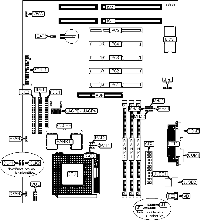
CONNECTIONS |
|||
| Purpose | Location |
Purpose | Location |
| AGP slot | AGP | IDE interface 1 | IDE1 |
| ATX power connector | ATX | IDE interface 2 | IDE2 |
| Chassis fan power | CFAN | 16-bit ISA slots | IS1 - IS2 |
| Serial port 1 | COM1 | PS/2 keyboard interface | J1 |
| Serial port 2 | COM2 | PS/2 mouse interface | J2 |
| Floppy drive interface | FDD1 | IR connector | JIR |
| Turbo LED | FPNL1/Pins 1 & 2 | USB port 1 | JUSB1 |
| Power LED & keylock | FPNL1/Pins 4 - 8 | USB port 2 | JUSB2 |
| Speaker | FPNL1/Pins 10 - 13 | PS/2 keyboard port | KB |
| Green PC connector | FPNL1/Pins 15 & 16 | Parallel port | LPT1 |
| Power switch | FPNL1/Pins 17 & 18 | 32-bit PCI slots | PC1 - PC5 |
| IRDA connector | FPNL1/Pins 19 - 23 | PS/2 mouse port | PS2 |
| IDE interface LED | FPNL1/Pins 24 & 25 | CPU fan power | PFAN |
| Reset switch | FPNL1/Pins 27 & 28 | Power fan power | VFAN |
| Turbo switch | FPNL1/Pins 30 - 32 | ||
USER CONFIGURABLE SETTINGS |
|||
Function |
Label |
Position |
|
» |
CMOS memory normal operation | BAT | Pins 1 & 2 closed |
| CMOS memory clear | BAT | Pins 2 & 3 closed | |
» |
Factory configured - do not alter | JAGP0 |
Pins 1 & 2 closed |
» |
Factory configured - do not alter | JAGP3 |
Pins 2 & 3 closed |
» |
Factory configured - do not alter | JAGP4 |
Pins 1 & 2 closed |
» |
Factory configured - do not alter | JTAG1 |
Pins 2 & 3 closed |
» |
Factory configured - do not alter | JVTA1 |
Pins 1 & 2 closed |
» |
Factory configured - do not alter | MHZ0 |
Pins 2 & 3 closed |
| Note: The location and size of jumpers JTAG1 and JVTA1 are not identified. | |||
DIMM CONFIGURATION |
|||
Size |
Bank 0 |
Bank 1 |
Bank 2 |
8MB |
(1) 1M x 64 |
None |
None |
16MB |
(1) 1M x 64 |
(1) 1M x 64 |
None |
16MB |
(1) 2M x 64 |
None |
None |
24MB |
(1) 1M x 64 |
(1) 1M x 64 |
(1) 1M x 64 |
32MB |
(1) 2M x 64 |
(1) 2M x 64 |
None |
32MB |
(1) 4M x 64 |
None |
None |
32MB |
(1) 2M x 64 |
(1) 1M x 64 |
(1) 1M x 64 |
48MB |
(1) 2M x 64 |
(1) 2M x 64 |
(1) 2M x 64 |
48MB |
(1) 4M x 64 |
(1) 1M x 64 |
(1) 1M x 64 |
64MB |
(1) 4M x 64 |
(1) 4M x 64 |
None |
64MB |
(1) 8M x 64 |
None |
None |
64MB |
(1) 4M x 64 |
(1) 2M x 64 |
(1) 2M x 64 |
80MB |
(1) 8M x 64 |
(1) 1M x 64 |
(1) 1M x 64 |
96MB |
(1) 4M x 64 |
(1) 4M x 64 |
(1) 4M x 64 |
96MB |
(1) 8M x 64 |
(1) 2M x 64 |
(1) 2M x 64 |
128MB |
(1) 8M x 64 |
(1) 8M x 64 |
None |
128MB |
(1) 16M x 64 |
None |
None |
128MB |
(1) 8M x 64 |
(1) 4M x 64 |
(1) 4M x 64 |
144MB |
(1) 16M x 64 |
(1) 1M x 64 |
(1) 1M x 64 |
160MB |
(1) 16M x 64 |
(1) 2M x 64 |
(1) 2M x 64 |
192MB |
(1) 8M x 64 |
(1) 8M x 64 |
(1) 8M x 64 |
192MB |
(1) 16M x 64 |
(1) 4M x 64 |
(1) 4M x 64 |
256MB |
(1) 16M x 64 |
(1) 16M x 64 |
None |
256MB |
(1) 32M x 64 |
None |
None |
256MB |
(1) 16M x 64 |
(1) 8M x 64 |
(1) 8M x 64 |
272MB |
(1) 32M x 64 |
(1) 1M x 64 |
(1) 1M x 64 |
288MB |
(1) 32M x 64 |
(1) 2M x 64 |
(1) 2M x 64 |
320MB |
(1) 32M x 64 |
(1) 4M x 64 |
(1) 4M x 64 |
384MB |
(1) 16M x 64 |
(1) 16M x 64 |
(1) 16M x 64 |
| Note: Board supports SDRAM memory. | |||
CACHE CONFIGURATION |
|
Size |
Bank 0 |
512KB |
(2) 64K x 32 |
1024KB |
(2) 128K x 32 |
CPU/PCI CLOCK SPEED SELECTION |
||
CPU speed |
JAGP1 |
JAGP2 |
60 - 75MHz |
Pins 2 & 3 closed |
Pins 2 & 3 closed |
75 - 83MHz |
Pins 1 & 2 closed |
Pins 1 & 2 closed |
90 - 100MHz |
Pins 2 & 3 closed |
Pins 1 & 2 closed |
CLOCK SPEED SELECTION |
|||
Clock Speed |
MHZ1 | MHZ2 | MHZ3 |
| 60MHz | Pins 2 & 3 closed | Pins 2 & 3 closed | Pins 2 & 3 closed |
| 66MHz | Pins 2 & 3 closed | Pins 2 & 3 closed | Pins 1 & 2 closed |
| 75MHz | Pins 2 & 3 closed | Pins 1 & 2 closed | Pins 2 & 3 closed |
| 83MHz | Pins 2 & 3 closed | Pins 1 & 2 closed | Pins 1 & 2 closed |
| 95MHz | Pins 1 & 2 closed | Pins 1 & 2 closed | Pins 2 & 3 closed |
| 100MHz | Pins 1 & 2 closed | Pins 1 & 2 closed | Pins 1 & 2 closed |
CPU MULTIPLIER SELECTION |
|||
Multiplier |
RAT1 | RAT2 | RAT3 |
1.5x |
Pins 1 & 2 closed | Pins 1 & 2 closed | Pins 1 & 2 closed |
2x |
Pins 2 & 3 closed | Pins 1 & 2 closed | Pins 2 & 3 closed |
2.5x |
Pins 2 & 3 closed | Pins 2 & 3 closed | Pins 1 & 2 closed |
3x |
Pins 1 & 2 closed | Pins 2 & 3 closed | Pins 1 & 2 closed |
| 3.5x | Pins 1 & 2 closed | Pins 1 & 2 closed | Pins 1 & 2 closed |
| 4x | Pins 2 & 3 closed | Pins 1 & 2 closed | Pins 2 & 3 closed |
| 4.5x | Pins 2 & 3 closed | Pins 2 & 3 closed | Pins 2 & 3 closed |
| 5x | Pins 1 & 2 closed | Pins 2 & 3 closed | Pins 2 & 3 closed |
| 5.5x | Pins 1 & 2 closed | Pins 1 & 2 closed | Pins 2 & 3 closed |
CPU VOLTAGE SELECTION (DUAL) |
|
Voltage |
VOL |
| 2.0V | Pins 3 & 4, 5 & 6, 7 & 8, 9 & 10 closed |
| 2.1V | Pins 1 & 2 closed |
| 2.2V | Pins 3 & 4 closed |
| 2.7V | Pins 1 & 2, 3 & 4, 5 & 6 closed |
| 2.8V | Pins 7 & 8 closed |
| 2.9V | Pins 1 & 2, 7 & 8 closed |
| 3.2V | Pins 5 & 6, 7 & 8 closed |
| 3.4V | Pins 3 & 4, 5 & 6, 7 & 8 closed |
CPU VOLTAGE SELECTION (SINGLE) |
|
Voltage |
VOL |
| 3.3V | Pins 1 & 2, 5 & 6, 7 & 8 closed |
| 3.5V | Pins 1 & 2, 3 & 4, 5 & 6, 7 & 8 closed |
BUS SPEED SELECTION |
|||
Setting |
CLK1 |
CLK2 |
|
| » | Bus speed set to match AGP |
Pins 2 & 3 closed |
Pins 1 & 2 closed |
Bus speed set to match CPU |
Pins 1 & 2 closed |
Pins 2 & 3 closed |
|