OCEAN INFORMATION SYSTEMS, INC.
HIPPO OP 486
| Device Type | Mainboard |
| Processor | 80486SX/80487SX/80486DX/80486DX2 |
| Processor Speed | 25/33/40/50MHz |
| Chip Set | Unidentified |
| Maximum Onboard Memory | 32MB |
| Cache | 256KB |
| BIOS | Unidentified |
| Dimensions | Unidentified |
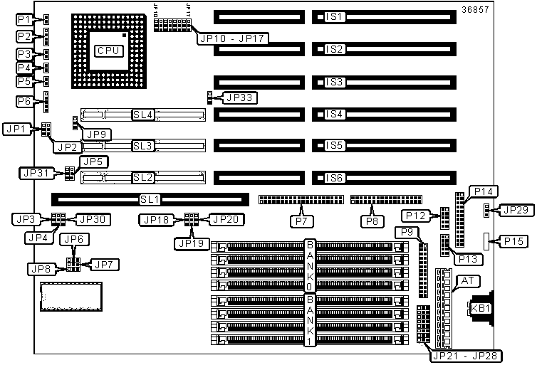
| I/O Options | 32-bit VESA local bus slots (3), 16-bit ISA slots (6), floppy drive interface, IDE interface, game interface, AT Keyboard port, parallel interface, serial interfaces (2), cache slot, AT power connector |
CONNECTIONS |
|||
| Purpose | Location |
Purpose | Location |
| AT power connector | AT | IDE interface | P7 |
| 16-bit ISA slots | IS1 - IS6 | Floppy drive interface | P8 |
| AT keyboard port | KB1 | Parallel interface | P9 |
| Reset switch | P1 | Serial interface 1 | P12 |
| Speaker | P2 | Serial interface 2 | P13 |
| Turbo LED | P3 | Game interface | P14 |
| Turbo switch | P4 | External battery connector | P15 |
| IDE interface LED | P5 | Cache slot | SL1 |
| Power LED & keylock | P6 | 32-bit VESA local bus slots | SL2 - SL4 |
USER CONFIGURABLE SETTINGS |
|||
Function |
Label |
Position |
|
| 1 WS VL-write cycle | JP1 | Pins 1 & 2 closed | |
| 0 WS VL-write cycle | JP1 | Pins 2 & 3 closed | |
» |
IDE wait state forced to 1 | JP2 |
Pins 2 & 3 closed |
| IDE wait state determined by JP1 setting | JP2 |
Pins 1 & 2 closed |
|
» |
Two cache banks installed | JP5 | Pins 2 & 3 closed |
| Single cache bank installed | JP5 | Pins 1 & 2 closed | |
| » | Color display mode | JP6 |
Pins 2 & 3 closed |
| Mono display mode | JP6 |
Pins 1 & 2 closed |
|
| » | EPROM installed | JP7 | Pins 1 & 2 closed |
| Flash ROM installed | JP7 | Pins 2 & 3 closed | |
» |
Factory configured - do not alter | JP8 | Pins 2 & 3 closed |
» |
Factory configured - do not alter | JP9 | Unidentified |
» |
Factory configured - do not alter | JP10 | Pins 2 & 3 closed |
» |
Factory configured - do not alter | JP11 | Pins 1 & 2 closed |
| IDE interface set as primary | JP13 | Pins 1 & 2 closed | |
| IDE interface set as secondary | JP13 | Pins 2 & 3 closed | |
» |
IDE interface cycle time > 840ns | JP16 | Pins 2 & 3 closed |
| IDE interface cycle time > 600ns | JP16 | Pins 1 & 2 closed | |
| » | On-board floppy drive interface enabled | JP21 |
Pins 1 & 2 closed |
| On-board floppy drive interface disabled | JP21 |
Pins 2 & 3 closed |
|
| » | On-board game interface enabled | JP22 |
Pins 1 & 2 closed |
| On-board game interface disabled | JP22 |
Pins 2 & 3 closed |
|
» |
On-board parallel interface enabled | JP23 |
Pins 1 & 2 closed |
|
On-board parallel interface disabled | JP23 |
Pins 2 & 3 closed |
| » | Parallel interface address set to LPT1 (378h) | JP24 |
Pins 1 & 2 closed |
| Parallel interface address set to LPT2 (278h) | JP24 |
Pins 2 & 3 closed |
|
| » | Serial interface 1 enabled | JP25 |
Pins 1 & 2 closed |
| Serial interface 1 disabled | JP25 | Pins 2 & 3 closed |
|
| » | Serial interface 1 address set to COM1 (3F8 - 3FFh) | JP26 | Pins 1 & 2 closed |
| Serial interface 1 address set to COM3 (3E8 - 3EFh) | JP26 | Pins 2 & 3 closed | |
| » | Serial interface 2 address set to COM2 (2F8 - 2FFh) | JP27 | Pins 1 & 2 closed |
| Serial interface 2 address set to COM4 (2E8 - 2EFh) | JP27 | Pins 2 & 3 closed | |
| » | Serial interface 2 enabled | JP28 |
Pins 1 & 2 closed |
| Serial interface 2 disabled | JP28 | Pins 2 & 3 closed |
|
» |
CMOS memory normal operation | JP29 |
Pins 1 & 2 closed |
| CMOS memory clear | JP29 |
Pins 2 & 3 closed |
|
| » | VL clock <= 33MHz | JP31 | Pins 2 & 3 closed |
| VL clock > 33MHz | JP31 | Pins 1 & 2 closed | |
» |
Factory configured - do not alter | JP33 | Pins 1 & 2 closed |
SIMM CONFIGURATION |
||
Size |
Bank 0 |
Bank 1 |
1MB |
(4) 256K x 32 |
None |
2MB |
(4) 256K x 32 |
(4) 256K x 32 |
4MB |
(4) 1M x 32 |
None |
5MB |
(4) 256K x 32 |
(4) 1M x 32 |
5MB |
(4) 1M x 32 |
(4) 256K x 32 |
8MB |
(4) 1M x 32 |
(4) 1M x 32 |
16MB |
(4) 4M x 32 |
None |
17MB |
(4) 256K x 32 |
(4) 4M x 32 |
17MB |
(4) 4M x 32 |
(4) 256K x 32 |
20MB |
(4) 1M x 32 |
(4) 4M x 32 |
20MB |
(4) 4M x 32 |
(4) 1M x 32 |
32MB |
(4) 4M x 32 |
(4) 4M x 32 |
CPU CLOCK SPEED SELECTION |
||||
CPU |
Clock speed |
JP3 |
JP4 |
JP30 |
DX25, DX2-50 |
25MHz |
Pins 1 & 2 closed | Pins 1 & 2 closed | Pins 2 & 3 closed |
DX33, DX2-66 |
33MHz |
Pins 2 & 3 closed | Pins 2 & 3 closed | Pins 2 & 3 closed |
DX40 |
40MHz |
Pins 1 & 2 closed | Pins 2 & 3 closed | Pins 2 & 3 closed |
DX50 |
50MHz |
Pins 2 & 3 closed | Pins 1 & 2 closed | Pins 1 & 2 closed |
CPU TYPE SELECTION |
||||
Type |
JP18 | JP19 | JP20 | |
| » | 486DX, 486DX2 | Pins 2 & 3 closed | Pins 1 & 2 closed | Pins 1 & 2 closed |
| 486SX | Pins 1 & 2 closed | Pins 2 & 3 closed | Pins 2 & 3 closed | |
IDE INTERFACE CONTROL |
|||
Setting |
JP12 | JP17 | |
» |
Enabled | Pins 1 & 2 closed | Pins 1 & 2 closed |
|
Disabled | Pins 2 & 3 closed | Pins 2 & 3 closed |
IDE CYCLE TIME SELECTION |
|||
Setting |
JP14 | JP15 | |
| » | > 480ns | Pins 2 & 3 closed | Pins 2 & 3 closed |
|
> 200ns | Pins 1 & 2 closed | Pins 1 & 2 closed |
|
> 240ns | Pins 1 & 2 closed | Pins 2 & 3 closed |
| > 383ns | Pins 2 & 3 closed | Pins 1 & 2 closed | |