DIGITAL VIEW COMPANY
AV-1280 (4163600-04)
| Card Type | Video card |
| Video Chip Set | Unidentified |
| Maximum Video Memory | Unidentified |
| Video Types Supported | SXGA, XGA, PAL, NTSC, SECAM |
| Highest Resolution Supported | 1280 x 1024 |
| Data Bus | None |
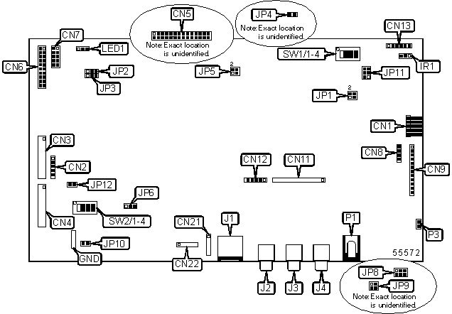
CONNECTIONS |
|||
Function |
Label |
Function |
Label |
| Audio connector | CN1 | Unidentified | CN21 |
| Alternate video input | CN2 | Unidentified | CN22 |
| Reserved | CN3 | Ground connector | GND |
| Reserved | CN4 | IR connector | IR1 |
| LCD panel connector A | CN5 | S-video in | J1 |
| LCD panel connector B | CN6 | Composite video in | J2 |
| LCD panel connector C | CN7 | Audio in - left channel | J3 |
| Auxilliary power connector | CN8 | Audio in - right channel | J4 |
| OSD switch | CN9 | LED connector | LED1 |
| Backlight inverter connector | CN11 | DC 12V power connector | P1 |
| Unidentified | CN12 | Alternative DC power connector | P3 |
| Reserved | CN13 | ||
USER CONFIGURABLE SETTINGS |
|||
Function |
Label |
Position |
|
» |
Factory configured - do not alter | JP1 | Unidentified |
| Inverter polarity control High = backlight on | JP3 | Pins 1 & 2 closed | |
| Inverter polarity control Low = backlight on | JP3 | Pins 2 & 3 closed | |
| +12V panel power voltage on CN7 enabled | JP4 | Closed | |
| +12V panel power voltage on CN7 disabled | JP4 | Open | |
» |
Factory configured - do not alter | JP5 | Unidentified |
| Panel voltage +3.3V selected | JP6 | Pins 1 & 2 closed | |
| Panel voltage +5V selected | JP6 | Pins 2 & 3 closed | |
| RS-232 logic level = +/-9V | JP8 | Pins 1 & 3, 2 & 4 closed | |
| RS-232 logic level = TTL level | JP8 | Pins 3 & 5, 4 & 6 closed | |
» |
Factory configured - do not alter | JP9 | Pins 1 & 3 closed |
» |
Factory configured - do not alter | JP9 | Pins 2 & 4 closed |
| +12V backlight power always enabled | JP10 | Open | |
| +12V backlight power controled by backlight switch | JP10 | Closed | |
» |
Factory configured - do not alter | JP11 | Unidentifed |
» |
Factory configured - do not alter | JP12 | Unidentified |
| Connected to SXGA panel | SW2/2 | Off | |
| Connected to LG LM181E1SXGA panel with 4106886-xx LVDS add-on board | SW2/2 | On | |
» |
Factory configured - do not alter | SW2/3 | Off |
| OSD volume control enabled | SW2/4 | On | |
| OSD volume control disabled | SW2/4 | Off | |
P ANEL SELECTION |
||||
S etting |
SW1/1 | SW1/2 | SW1/3 | SW1/4 |
S XGA |
Off | On | On | Off |
X GA (dual pixel/clock) |
On | Off | On | On |
| XGA (single pixel/clock) | Off | Off | On | On |
INVERTER SIGNAL LEVEL SELECTION |
|
| Settings | JP2 |
| High = +12V | Pins 1 & 2 closed |
| High = +5V | Pins 2 & 3 closed |
| High = open collector | Open |
MISCELLANEOUS TECHNICAL NOTES |
S W2/1 is used to change the clock phase. Switch SW2/1 on and off to obtain best image stability. |