SBE, INC.
SCI-530C
| Card Type | Serial communication interface module |
| Chip Set | Unidentified |
| Maximum Modem Rate | 4Mbps |
| Data Modulation Protocol | EIA-232 -D, EIA-422, EIA-449, EIA-530, V.35, X.21 |
| Data Bus | Propietary |
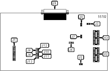
CONNECTIONS |
|||
Function |
Label |
Function |
Label |
| 20-pin connector to host board | J 1 |
25-pin D type connector | J9 |
USER CONFIGURABLE SETTINGS |
|||
Setting |
Label |
Position |
|
| » | Host to DTE delay line signal disabled | J2 | Closed |
| Host to DTE delay line signal enabled | J2 | Open | |
| » | DTE to Host delay line signal disabled | J3 | Closed |
| DTE to Host delay line signal enabled | J3 | Open | |
| » | Test mode is Low (-5v) | J5 | Pins 2 & 3 closed |
| Test mode is High (+5v) | J5 | Pins 1 & 2 closed | |
| GROUNDING OPTIONS | |||
Function |
J7 |
J8 |
|
| » | J9 connected to frame ground and circuit ground (100 resistor) | Open | Closed |
| J9 with no ground | Closed | Open | |
| J9 connected to frame ground and circuit ground (bypass 100 resistor) | Closed | Closed | |
| J9 with no ground | Open | Open | |
| SINGLE CLOCK SOURCE | |||||||
Source |
J4 |
J6 |
J10 |
J11 | J12 | J13 |
|
| » | Host board (DCE) | Open | Closed | 1 & 2, 3 & 4 | Closed | Closed | Open |
| DTE device | Closed | Closed | 1 & 3, 2 & 4 | Open | Closed | Open | |
| Opcional oscillator | Open | Closed | 1 & 3, 2 & 4 | Closed | Closed | Closed | |
| Note:
J11 should be kept Open and J12 should be kept Closed when configuring SCI-530T. Note: Pins designated are in the closed position. |
|||||||
| DUAL CLOCK SOURCE | |||||||
Source |
J4 |
J6 |
J10 |
J11 | J12 | J13 |
|
| » | DCE supplies timing to DTE device | N/A | N/A | 1 & 2, 3 & 4 | Open | Closed | Open |
| Oscillator supplies timing to DTE device | N/A | N/A | 1 & 3, 2 & 4 | Open | Closed | Closed | |
| DTE supplies timing to DCE device | Closed | Open | N/A | N/A | N/A | N/A | |
| Note:
J11 should be kept Open and J12 should be kept Closed when configuring SCI-530T. Note: Pins designated are in the closed position. |
|||||||