ASUS COMPUTER INTERNATIONAL
P2-99B (REV. 1.01)
| Device Type | Mainboard |
| Processor | Pentium II/Pentium III/Celeron |
| Processor Speed | 233/266/300/333/350/366/400/433/450/466/500/550MHz |
| Chip Set | Intel 440ZX |
| Maximum Onboard Memory | 512MB (SDRAM supported) |
| Cache | 0/128/256/512KB (located on the CPU) |
| BIOS | Award |
| Dimensions | 221mm x 229mm |
| I/O Options | 32-bit PCI slots (3), floppy drive interface, green PC connector, IDE interfaces (2), PS/2 mouse interface, serial interfaces (2), IR connector, USB connectors (2), ATX power connector, AGP slot, Wake-on-LAN connector, Wake-on-ring connector, SB-Link connector, SMBus connector |
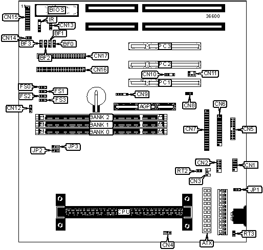
CONNECTIONS |
|||
| Purpose | Location |
Purpose | Location |
| AGP slot | AGP |
Wake-on-ring connector | CN13 |
| ATX power connector | ATX |
IDE interface LED | CN14 |
| Serial interface 1 | CN1 | Power LED & keylock | CN15/Pins 1-5 |
| Serial interface 2 | CN2 | Speaker | CN15/Pins 7-10 |
| Power fan | CN3 | Message LED | CN15/Pins 12 & 13 |
| CPU fan power | CN4 | Green PC connector | CN15/Pins 14 & 15 |
| USB/IR/Mouse interface | CN5 | Soft off power supply | CN15/Pins 16 & 17 |
| Parallel interface | CN6 | Reset switch | CN15/Pins 19 & 20 |
| Floppy drive interface | CN7 | IDE interface 2 | CN16 |
| Wake-on-LAN connector | CN8 | IDE interface 1 | CN17 |
| SMBus connector | CN9 | IR connector | IR |
| Chassis intrusion sensor connector | CN10 | 32-bit PCI slots | PC1 - PC3 |
| SB-Link connector | CN11 | CPU thermal sesor connector | RT2 |
| Chassis fan power | CN12 | Power supply thermal sensor connector | RT3 |
USER CONFIGURABLE SETTINGS |
|||
Function |
Label |
Position |
|
» |
Keyboard power on disabled | JP1 | Pins 1 & 2 Closed |
| Keyboard power on enabled | JP1 | Pins 2 & 3 Closed | |
| » | I/O voltage 3.50V | JP2 | Pins 2 & 3 Closed |
|
I/O voltage 3.66V | JP2 | Pins 1 & 2 Closed |
| » | Core voltage normal | JP3 | Pins 2 & 3 Closed |
| Core voltage test | JP3 | Pins 1 & 2 Closed | |
| DIMM CONFIGURATION | |||
Size |
Bank 0 |
Bank 1 |
Bank 2 |
8MB |
(1) 1M x 64 |
None |
None |
16MB |
(1) 1M x 64 |
(1) 1M x 64 |
None |
16MB |
(1) 2M x 64 |
None |
None |
24MB |
(1) 1M x 64 |
(1) 1M x 64 |
(1) 1M x 64 |
32MB |
(1) 2M x 64 |
(1) 2M x 64 |
None |
32MB |
(1) 4M x 64 |
None |
None |
32MB |
(1) 2M x 64 |
(1) 1M x 64 |
(1) 1M x 64 |
48MB |
(1) 2M x 64 |
(1) 2M x 64 |
(1) 2M x 64 |
48MB |
(1) 4M x 64 |
(1) 1M x 64 |
(1) 1M x 64 |
64MB |
(1) 4M x 64 |
(1) 4M x 64 |
None |
64MB |
(1) 8M x 64 |
None |
None |
64MB |
(1) 4M x 64 |
(1) 2M x 64 |
(1) 2M x 64 |
80MB |
(1) 8M x 64 |
(1) 1M x 64 |
(1) 1M x 64 |
96MB |
(1) 4M x 64 |
(1) 4M x 64 |
(1) 4M x 64 |
96MB |
(1) 8M x 64 |
(1) 2M x 64 |
(1) 2M x 64 |
128MB |
(1) 8M x 64 |
(1) 8M x 64 |
None |
128MB |
(1) 16M x 64 |
None |
None |
128MB |
(1) 8M x 64 |
(1) 4M x 64 |
(1) 4M x 64 |
144MB |
(1) 16M x 64 |
(1) 1M x 64 |
(1) 1M x 64 |
160MB |
(1) 16M x 64 |
(1) 2M x 64 |
(1) 2M x 64 |
192MB |
(1) 8M x 64 |
(1) 8M x 64 |
(1) 8M x 64 |
192MB |
(1) 16M x 64 |
(1) 4M x 64 |
(1) 4M x 64 |
256MB |
(1) 16M x 64 |
(1) 16M x 64 |
None |
256MB |
(1) 32M x 64 |
None |
None |
256MB |
(1) 16M x 64 |
(1) 8M x 64 |
(1) 8M x 64 |
272MB |
(1) 32M x 64 |
(1) 1M x 64 |
(1) 1M x 64 |
288MB |
(1) 32M x 64 |
(1) 2M x 64 |
(1) 2M x 64 |
320MB |
(1) 32M x 64 |
(1) 4M x 64 |
(1) 4M x 64 |
384MB |
(1) 16M x 64 |
(1) 16M x 64 |
(1) 16M x 64 |
384MB |
(1) 32M x 64 |
(1) 8M x 64 |
(1) 8M x 64 |
512MB |
(1) 32M x 64 |
(1) 32M x 64 |
None |
512MB |
(1) 32M x 64 |
(1) 16M x 64 |
(1) 16M x 64 |
| Note: Board supports SDRAM memory. | |||
CACHE CONFIGURATION |
| Note: 256KB/512KB cache is located on the Pentium II/Pentium III CPU. 128KB cache is located on the Celeron 300A and greater CPU. |
CPU SPEED SELECTION (CELERON) |
||||||
CPU speed |
Clock speed |
Multiplier |
FS0 |
FS1 |
FS2 | FS3 |
266MHz |
66MHz |
4x |
1 & 2 | 1 & 2 | 2 & 3 | 2 & 3 |
300MHz |
66MHz |
4.5x |
1 & 2 | 1 & 2 | 2 & 3 | 2 & 3 |
333MHz |
66MHz |
5x |
1 & 2 | 1 & 2 | 2 & 3 | 2 & 3 |
366MHz |
66MHz |
5.5x |
1 & 2 | 1 & 2 | 2 & 3 | 2 & 3 |
| 400MHz | 66MHz | 6x | 1 & 2 | 1 & 2 | 2 & 3 | 2 & 3 |
| 433MHz | 66MHz | 6.5x | 1 & 2 | 1 & 2 | 2 & 3 | 2 & 3 |
| 466MHz | 66MHz | 7x | 1 & 2 | 1 & 2 | 2 & 3 | 2 & 3 |
Note: Pins designated should be in the closed position. |
||||||
CPU SPEED SELECTION (CELERON CONT) |
||||||
CPU speed |
Clock speed |
Multiplier |
BF0 |
BF1 |
BF2 | BF3 |
266MHz |
66MHz |
4x |
2 & 3 | 2 & 3 | 1 & 2 | 2 & 3 |
300MHz |
66MHz |
4.5x |
1 & 2 | 2 & 3 | 1 & 2 | 2 & 3 |
333MHz |
66MHz |
5x |
2 & 3 | 1 & 2 | 1 & 2 | 2 & 3 |
366MHz |
66MHz |
5.5x |
1 & 2 | 1 & 2 | 1 & 2 | 2 & 3 |
| 400MHz | 66MHz | 6x | 2 & 3 | 2 & 3 | 2 & 3 | 1 & 2 |
| 433MHz | 66MHz | 6.5x | 1 & 2 | 2 & 3 | 2 & 3 | 1 & 2 |
| 466MHz | 66MHz | 7x | 2 & 3 | 1 & 2 | 2 & 3 | 1 & 2 |
| Note: Pins designated should be in the closed position. | ||||||
CPU SPEED SELECTION (PENTIUM II) |
||||||
CPU speed |
Clock speed |
Multiplier |
FS0 |
FS1 |
FS2 | FS3 |
| 233MHz | 66MHz | 3.5x | 1 & 2 | 1 & 2 | 2 & 3 | 2 & 3 |
266MHz |
66MHz |
4x |
1 & 2 | 1 & 2 | 2 & 3 | 2 & 3 |
300MHz |
66MHz |
4.5x |
1 & 2 | 1 & 2 | 2 & 3 | 2 & 3 |
333MHz |
66MHz |
5x |
1 & 2 | 1 & 2 | 2 & 3 | 2 & 3 |
350MHz |
100MHz |
3.5x |
1 & 2 | 1 & 2 | 1 & 2 | 2 & 3 |
| 400MHz | 100MHz | 4x | 1 & 2 | 1 & 2 | 1 & 2 | 2 & 3 |
| 450MHz | 100MHz | 4.5x | 1 & 2 | 1 & 2 | 1 & 2 | 2 & 3 |
Note: Pins designated should be in the closed position. |
||||||
CPU SPEED SELECTION (PENTIUM II CONT) |
||||||
CPU speed |
Clock speed |
Multiplier |
BF0 |
BF1 |
BF2 | BF3 |
| 233MHz | 66MHz | 3.5x | 1 & 2 | 1 & 2 | 2 & 3 | 2 & 3 |
266MHz |
66MHz |
4x |
2 & 3 | 2 & 3 | 1 & 2 | 2 & 3 |
300MHz |
66MHz |
4.5x |
1 & 2 | 2 & 3 | 1 & 2 | 2 & 3 |
333MHz |
66MHz |
5x |
2 & 3 | 1 & 2 | 1 & 2 | 2 & 3 |
350MHz |
100MHz |
3.5x |
1 & 2 | 1 & 2 | 2 & 3 | 2 & 3 |
| 400MHz | 100MHz | 4x | 2 & 3 | 2 & 3 | 1 & 2 | 2 & 3 |
| 450MHz | 100MHz | 4.5x | 1 & 2 | 2 & 3 | 1 & 2 | 2 & 3 |
Note: Pins designated should be in the closed position. |
||||||
CPU SPEED SELECTION (PENTIUM III) |
||||||
CPU speed |
Clock speed |
Multiplier |
FS0 |
FS1 |
FS2 | FS3 |
450MHz |
100MHz |
4.5x |
1 & 2 | 1 & 2 | 1 & 2 | 2 & 3 |
| 500MHz | 100MHz | 5x | 1 & 2 | 1 & 2 | 1 & 2 | 2 & 3 |
| 550MHz | 100MHz | 5.5x | 1 & 2 | 1 & 2 | 1 & 2 | 2 & 3 |
Note: Pins designated should be in the closed position. |
||||||
CPU SPEED SELECTION (PENTIUM III CONT) |
||||||
CPU speed |
Clock speed |
Multiplier |
BF0 |
BF1 |
BF2 | BF3 |
450MHz |
100MHz |
4.5x |
1 & 2 | 2 & 3 | 1 & 2 | 2 & 3 |
| 500MHz | 100MHz | 5x | 2 & 3 | 1 & 2 | 1 & 2 | 2 & 3 |
| 550MHz | 100MHz | 5.5x | 1 & 2 | 1 & 2 | 1 & 2 | 2 & 3 |
Note: Pins designated should be in the closed position. |
||||||