CHAINTECH COMPUTER COMPANY, LTD.
CT-5RSA2
| Device Type | Mainboard |
| Processor | CX 6X86/IBM 6X86/CX 6X86L/IBM 6X86L/CX 6X86MX/IBM 6X86MX/CX M2/AM K5/AM K6/AM K6-2/Pentium/Pentium MMX/IDT Winchip C6/IDT Winchip 2 |
| Processor Speed | 133/150/166/180/200/225/233/240/266/300/333/400MHz |
| Chip Set | ALI Aladdin |
| Audio Chip Set | ESS |
| Maximum Onboard Memory | 256MB (EDO SDRAM supported) |
| Maximum Audio Memory | Unidentified |
| Cache | 1024KB |
| BIOS | Award |
| Dimensions | 244mm x 220mm |
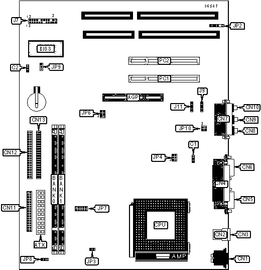
| I/O Options | 32-bit PCI slots (2), floppy drive interface, game port, green PC connector, IDE interfaces (2), parallel port, PS/2 mouse port, serial ports (2), IR connector, USB connectors (2), ATX power connector, AGP slot, line in, line out, microphone in, audio in - CD-ROMs (2) |
CONNECTIONS |
|||
| Purpose | Location |
Purpose | Location |
| AGP slot | AGP |
Microphone in | CN10 |
| ATX power connector | ATX |
Floppy drive interface | CN11 |
| Aux in connector | J9 | IDE interface 1 | CN12 |
| Audio in - CD-ROM | J11 | IDE interface 2 | CN13 |
| CPU fan power | C1 | Turbo LED | J7/Pins 1 & 2 |
| System fan power | C2 | Green PC connector | J7/Pins 4 & 5 |
| PS/2 mouse port | CN1 | Green PC LED | J7/Pins 6 & 7 |
| USB connector 1 | CN2 | Reset switch | J7/Pins 9 & 10 |
| USB connector 2 | CN3 | IDE interface LED | J7/Pins 11 & 12 |
| Parallel port | CN4 | Over-ride power connector | J7/Pins 13 & 14 |
| Serial port 1 | CN5 | Speaker | J7/Pins 15-18 |
| Serial port 2 | CN6 | Power LED & keylock | J7/Pins 20-24 |
| Game port | CN7 | IR connector | JP2 |
| Line out | CN8 | 32-bit PCI slots | PC1 - PC2 |
| Line in | CN9 | ||
USER CONFIGURABLE SETTINGS |
|||
Function |
Label |
Position |
|
|
CPU I/O voltage 3.45V | JP3 | Closed |
| CPU I/O voltage 3.52V | JP3 | Open | |
| » | Power failure recovery off | JP8 | Pins 2 & 3 Closed |
| Pwer failure recovery on | JP8 | Pins 1 & 2 Closed | |
| » | CMOS memory normal operation | JP9 | Pins 1 & 2 Closed |
|
CMOS memory Clear | JP9 | Pins 2 & 3 Closed |
| » | Volume selection up | JP10 | Pins 1 & 2 Closed |
| Volume selection down | JP10 | Pins 3 & 4 Closed | |
DIMM CONFIGURATION |
||
Size |
Bank 0 |
Bank 1 |
16MB |
(1) 2MB x 64 |
None |
32MB |
(1) 4MB x 64 |
None |
32MB |
(1) 2MB x 64 |
(1) 2MB x 64 |
48MB |
(1) 4MB x 64 |
(1) 2MB x 64 |
64MB |
(1) 8MB x 64 |
None |
64MB |
(1) 4MB x 64 |
(1) 4MB x 64 |
80MB |
(1) 8MB x 64 |
(1) 2MB x 64 |
96MB |
(1) 8MB x 64 |
(1) 4MB x 64 |
128MB |
(1) 16MB x 64 |
None |
128MB |
(1) 8MB x 64 |
(1) 8MB x 64 |
144MB |
(1) 16MB x 64 |
(1) 2MB x 64 |
160MB |
(1) 16MB x 64 |
(1) 4MB x 64 |
192MB |
(1) 16MB x 64 |
(1) 8MB x 64 |
256MB |
(1) 16MB x 64 |
(1) 16MB x 64 |
| Note: Board supports EDO SDRAM memory. | ||
CACHE CONFIGURATION |
| Note: Location and configuration of cache memory is unidentified |
| CPU SPEED SELECTION (PENTIUM) | ||||
CPU speed |
Clock speed |
Multiplier |
JP6 |
JP4 |
133MHz |
66MHz |
2x |
Pins 3 & 4, 5 & 6 | Pins 1 & 2 |
166MHz |
66MHz |
2.5x |
Pins 3 & 4, 5 & 6 | Pins 1 & 2, 3 & 4 |
200MHz |
66MHz |
3x |
Pins 3 & 4, 5 & 6 | Pins 3 & 4 |
Note: Pins designated should be in the closed position. |
||||
CPU SPEED SELECTION (PENTIUM MMX) |
||||
CPU speed |
Clock speed |
Multiplier |
JP6 |
JP4 |
166MHz |
66MHz |
2.5x |
Pins 3 & 4, 5 & 6 | Pins 1 & 2, 3 & 4 |
200MHz |
66MHz |
3x |
Pins 3 & 4, 5 & 6 | Pins 3 & 4 |
| 233MHz | 66MHz | 3.5 | Pins 3 & 4, 5 & 6 | Open |
Note: Pins designated should be in the closed position. |
||||
CPU SPEED SELECTION (CX 6X86/IBM 6X86) |
||||
CPU speed |
Clock speed |
Multiplier |
JP6 |
JP4 |
133MHz |
66MHz |
2x |
Pins 3 & 4, 5 & 6 | Pins 1 & 2 |
150MHz |
75MHz |
2x |
Pins 1 & 2, 3 & 4 | Pins 1 & 2 |
Note: Pins designated should be in the closed position. |
||||
CPU SPEED SELECTION (CX 6X86L/IBM 6X86L) |
||||
CPU speed |
Clock speed |
Multiplier |
JP6 |
JP4 |
133MHz |
66MHz |
2x |
Pins 3 & 4, 5 & 6 | Pins 1 & 2 |
150MHz |
75MHz |
2x |
Pins 1 & 2, 3 & 4 | Pins 1 & 2 |
Note: Pins designated should be in the closed position. |
||||
CPU SPEED SELECTION (CX 6X86MX/IBM 6X86MX) |
||||
CPU speed |
Clock speed |
Multiplier |
JP6 |
JP4 |
166MHz |
66MHz | 2x | Pins 3 & 4, 5 & 6 | Pins 1 & 2 |
200MHz |
66MHz | 2.5x | Pins 3 & 4, 5 & 6 | Pins 1 & 2, 3 & 4 |
| 200MHz | 75MHz | 2x | Pins 1 & 2, 3 & 4 | Pins 1 & 2 |
| 233MHz | 75MHz | 2.5x | Pins 1 & 2, 3 & 4 | Pins 1 & 2, 3 & 4 |
| 233MHz | 83MHz | 2x | Pins 3 & 4 | Pins 1 & 2 |
| 266MHz | 83MHz | 2.5x | Pins 3 & 4 | Pins 1 & 2, 3 & 4 |
Note: Pins designated should be in the closed position. |
||||
CPU SPEED SELECTION (CX MII) |
||||
CPU speed |
Clock speed |
Multiplier |
JP6 |
JP4 |
300MHz |
66MHz |
3.5x |
Pins 3 & 4, 5 & 6 | Open |
300MHz |
75MHz |
3x |
Pins 1 & 2, 3 & 4 | Pins 3 & 4 |
Note: Pins designated should be in the closed position. |
||||
CPU SPEED SELECTION (AM K5) |
||||
CPU speed |
Clock speed |
Multiplier |
JP6 |
JP4 |
166MHz |
66MHz |
2.5x |
Pins 3 & 4, 5 & 6 | Pins 1 & 2, 3 & 4 |
Note: Pins designated should be in the closed position. |
||||
CPU SPEED SELECTION (AM K6) |
||||
CPU speed |
Clock speed |
Multiplier |
JP6 |
JP4 |
166MHz |
66MHz |
2.5x |
Pins 3 & 4, 5 & 6 | Pins 1 & 2, 3 & 4 |
200MHz |
66MHz |
3x |
Pins 3 & 4, 5 & 6 | Pins 3 & 4 |
| 233MHz | 66MHz | 3.5x | Pins 3 & 4, 5 & 6 | Open |
| 266MHz | 66MHz | 4x | Pins 3 & 4, 5 & 6 | Pins 1 & 2, 5 & 6 |
Note: Pins designated should be in the closed position. |
||||
CPU SPEED SELECTION (AM K6-2) |
||||
CPU speed |
Clock speed |
Multiplier |
JP6 |
JP4 |
266MHz |
66MHz |
4x |
Pins 3 & 4, 5 & 6 | Pins 1 & 2, 5 & 6 |
300MHz |
100MHz |
3x |
Open | Pins 3 & 4 |
| 333MHz | 95MHz | 3.5x | Pins 1 & 2 | Open |
| 400MHz | 100MHz | 4x | Open | Pins 1 & 2, 5 & 6 |
Note: Pins designated should be in the closed position. |
||||
CPU SPEED SELECTION (IDT WINCHIP C6) |
||||
CPU speed |
Clock speed |
Multiplier |
JP6 |
JP4 |
180MHz |
66MHz |
3x |
Pins 3 & 4, 5 & 6 | Pins 3 & 4 |
225MHz |
75MHz |
3x |
Pins 1 & 2, 3 & 4 | Pins 3 & 4 |
Note: Pins designated should be in the closed position. |
||||
CPU SPEED SELECTION (IDT WINCHIP 2) |
||||
CPU speed |
Clock speed |
Multiplier |
JP6 |
JP4 |
240MHz |
60MHz |
4x |
Pins 1 & 2, 3 & 4, 5 & 6 | Pins 1 & 2, 5 & 6 |
Note: Pins designated should be in the closed position. |
||||
CPU CORE VOLTAGE SETTINGS |
|
Voltage |
JP7 |
1.7 |
Pins 7& 8, 9 & 10 Closed |
1.8 |
Pins 3 & 4, 7 & 8, 9 & 10 Closed |
| 1.9 | Pins 5 & 6, 7 & 8, 9 & 10 Closed |
| 2.0 | Pins 3 & 4, 5 & 6, 7 & 8, 9 & 10 Closed |
| 2.1 | Pins 1 & 2 Closed |
| 2.2 | Pins 3 & 4 Closed |
| 2.3 | Pins 1 & 2, 3 & 4 Closed |
| 2.4 | Pins 5 & 6 Closed |
| 2.5 | Pins 1 & 2, 5 & 6 Closed |
| 2.6 | Pins 3 & 4, 5 & 6 Closed |
| 2.7 | Pins 1 & 2, 3 & 4, 5 & 6 Closed |
| 2.8 | Pins 7 & 8 Closed |
| 2.9 | Pins 1 & 2, 7 & 8 Closed |
| 3.0 | Pins 3 & 4, 7 & 8 Closed |
| 3.1 | Pins 1 & 2, 3 & 4, 7 & 8 Closed |
| 3.2 | Pins 3 & 4, 5 & 6 Closed |
| 3.3 | Pins 1 & 2, 5 & 6, 7 & 8 Closed |
| 3.4 | Pins 3 & 4, 5 & 6, 7 & 8 Closed |
| 3.5 | Pins 1 & 2, 3 & 4, 5 & 6, 7 & 8 Closed |