SIGNATEC, INC.
DAC200
|
Card Type |
Multi-I/O card |
|
Chip Set |
Unidentified |
|
I/O Options |
Serial ports (2), analog out, digital out, trigger/gate out, clock in |
|
Data Bus |
16-bit ISA |
|
CONNECTIONS |
|||
|
Function |
Label |
Function |
Label |
|
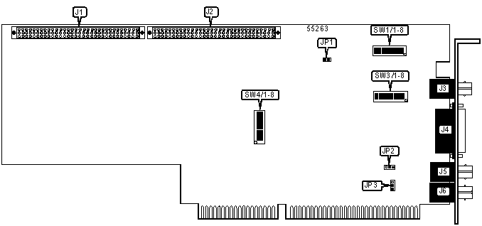
Signatec Auxiliary Bus (SAB) interface |
J1 |
Digital out |
J4 |
|
Signatec Auxiliary Bus (SAB) interface |
J2 |
Trigger/Gate out |
J5 |
|
Analog out |
J3 |
Clock in |
J6 |
|
USER CONFIGURABLE SETTINGS |
|||
|
Setting |
Label |
Position |
|
| » |
Adjust gain at high frequency |
JP1 |
Closed |
|
Fixed gain |
JP1 |
Open |
|
| » |
Ground termination |
JP2 |
Pins 2 & 3 closed |
|
-2V termination |
JP2 |
Pins 1 & 2 closed |
|
| » |
Capacitive coupled external clock |
JP3 |
Pins 1 & 2 closed |
|
ECL direct coupled external clock |
JP3 |
Pins 2 & 3 closed |
|
| » |
Factory configured - do not alter |
SW1/1 |
Unidentified |
| » |
Factory configured - do not alter |
SW1/2 |
Unidentified |
| » |
Factory configured - do not alter |
SW1/4 |
Unidentified |
| » |
Factory configured - do not alter |
SW1/6 |
Unidentified |
| » |
Factory configured - do not alter |
SW1/7 |
Unidentified |
| » |
Factory configured - do not alter |
SW2 |
Unidentified |
|
Direct coupled output select |
SW3/1 |
On |
|
|
Capacitive coupled output select |
SW3/1 |
Off |
|
| » |
Factory configured - do not alter |
SW3/2 |
Unidentified |
| » |
Factory configured - do not alter |
SW3/4 |
Unidentified |
| » |
Factory configured - do not alter |
SW3/6 |
Unidentified |
| » |
Factory configured - do not alter |
SW3/7 |
Unidentified |
|
Note: The location of SW2 is unidentified. |
|||
|
SIGNAL BANDWIDTH SELECTION |
||||||
|
Setting |
SW1/3 |
SW1/5 |
SW1/8 |
SW3/3 |
SW3/5 |
SW3/8 |
|
Maximum |
Off |
On |
Off |
Off |
On |
Off |
|
80MHz |
Off |
On |
Off |
Off |
On |
Off |
|
40MHz |
Off |
Off |
On |
Off |
Off |
On |
|
BASE I/O ADDRESS SELECTION |
||||||||
|
Setting |
SW4/1 |
SW4/2 |
SW4/3 |
SW4/4 |
SW4/5 |
SW4/6 |
SW4/7 |
|
|
0h |
On |
On |
On |
On |
On |
On |
On |
|
|
8h |
On |
On |
On |
On |
On |
On |
Off |
|
|
10h |
On |
On |
On |
On |
On |
Off |
On |
|
|
18h |
On |
On |
On |
On |
On |
Off |
Off |
|
|
20h |
On |
On |
On |
On |
Off |
On |
On |
|
| » |
320h |
Off |
Off |
On |
On |
Off |
On |
On |
|
3D8 |
Off |
Off |
Off |
Off |
On |
Off |
Off |
|
|
3E0 |
Off |
Off |
Off |
Off |
Off |
On |
On |
|
|
3E8 |
Off |
Off |
Off |
Off |
Off |
On |
Off |
|
|
3F0 |
Off |
Off |
Off |
Off |
Off |
Off |
On |
|
|
3F8 |
Off |
Off |
Off |
Off |
Off |
Off |
Off |
|
|
Note: A total of 127 base address settings are available. The switches are a binary representation of the decimal memory addresses. SW4/1 is the Most Significant Bit and switch SW4/7 is the Least Significant Bit. The switches have the following decimal values: SW4/7=8 SW4/6=16, SW4/5=32, SW4/4=64, SW4/3=128, SW4/2=256, SW4/1=512. Turn off the switches and add the values of the switches to obtain the correct memory address. (Off=1, On=0) |
||||||||