 .
.
ADVANTECH CO., LTD.
PCL-838
|
Card Type |
Stepping Motor Control card |
|
Chip Set |
Unidentified |
|
Maximum Onboard Memory |
Unidentified |
|
I/O Options |
20-pin termination connectors (2), 37-pin connector |
|
Data Bus |
8-bit ISA |
|
Card Size |
Full-length, full-height |
.
|
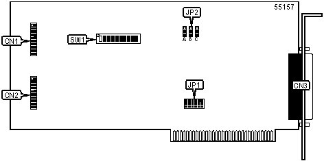
CONNECTIONS |
|||
|
Function |
Label |
Function |
Label |
|
Digital out |
CN1 |
37-pin connector |
CN3 |
|
Digital in |
CN2 |
||
|
USER CONFIGURABLE SETTINGS |
|||
|
Function |
Label |
Position |
|
| » |
Factory configured - do not alter |
JP1 |
Unidentified |
|
BASE I/O ADDRESS SELECTION |
||||||
|
Setting |
SW1/4 |
SW1/5 |
SW1/6 |
SW1/7 |
SW1/8 |
|
|
200h |
On |
On |
On |
On |
On |
|
|
210h |
Off |
On |
On |
On |
On |
|
| » |
2E0h |
On |
Off |
Off |
Off |
On |
|
300h |
On |
On |
On |
On |
Off |
|
|
3F0h |
Off |
Off |
Off |
Off |
Off |
|
|
Note: A total of 64 base address settings are available. The switches are a binary representation of the decimal memory addresses. SW1/8 is the Most Significant Bit and switch SW1/4 is the Least Significant Bit. The switches have the following decimal values: SW1/8=256, SW1/7=224, SW1/6=208, SW1/5=172, SW1/4=148. Turn off the switches and add the values of the switches to obtain the correct memory address. (Off=1, On=0) |
||||||
|
WAIT STATE SELECTION |
|||
|
Setting |
SW1/9 |
SW1/10 |
|
| » |
0 |
On |
On |
|
2 |
Off |
On |
|
|
4 |
On |
Off |
|
|
6 |
Off |
Off |
|
|
CHANNEL 1 DRIVER INITIAL SIGNAL LEVEL SETTING |
||
|
Setting |
JP2/A |
|
| » |
Normal |
Pins 1 & 2 |
|
Inverted |
Pins 2 & 3 |
|
|
CHANNEL 2 DRIVER INITIAL SIGNAL LEVEL SETTING |
||
|
Setting |
JP2/B |
|
| » |
Normal |
Pins 1 & 2 |
|
Inverted |
Pins 2 & 3 |
|
|
CHANNEL 3 DRIVER INITIAL SIGNAL LEVEL SETTING |
||
|
Setting |
JP2/C |
|
| » |
Normal |
Pins 1 & 2 |
|
Inverted |
Pins 2 & 3 |
|
|
DIRECTION CONTROL MODE |
|||
|
Mode |
SW1/1 |
SW1/2 |
SW1/3 |
|
One-pulse |
On |
On |
On |
|
Two-pulse |
Off |
Off |
Off |