INDUSTRIAL COMPUTER SOURCE
ISO-COM485/2
| Card Type | Serial card |
| I/O Options | serial ports (2) |
| Data Bus | 16-bit ISA |
| Card Size | Full-length |
CONNECTIONS |
|||
Function |
Label |
Function |
Label |
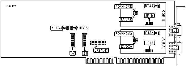
| 9-pin connector | J1 |
9—pin connector | J2 |
RTS CONTROL: COM A |
|
Function |
RTSA |
| For RS-485 operation, allows the state of the RTS line to be controlled by the UART for COM A | Closed |
RTS CONTROL: COM B |
|
Function |
RTSB |
| For RS-485 operation, allows the state of the RTS line to be controlled by the UART for COM B | Closed |
AUTO SETTING: COM A |
|
Function |
AUTOA |
| Allows the ACE data buffer to automatically control transmitter drivers for COM A. Use the AUTO mode when operating with Windows programs. | Closed |
AUTO SETTING: COM B |
|
Function |
AUTOB |
| Allows the ACE data buffer to automatically control transmitter drivers for COM B. Use the AUTO mode when operating with Windows programs. | Closed |
SIMPLEX/DUPLEX SETTING: COM A |
|
Function |
SX/DXA |
| Enables SIMPLEX mode, one-way communication, for COM A | Pins 1 & 2 closed |
| Enables DUPLEX mode, two-way communication, for COM A | Pins 2 & 3 closed |
SIMPLEX/DUPLEX SETTING: COM B |
|
Function |
SX/DXB |
| Enables SIMPLEX mode, one-way communication, for COM B | Pins 1 & 2 closed |
| Enables DUPLEX mode, two-way communication, for COM B | Pins 2 & 3 closed |
HALF/FULL DUPLEX SETTING: COM A |
|
Function |
HDX/FDXA |
| Enables FULL DUPLEX mode, allowing simultaneous two-way communications for COM A | Pins 2 & 3 closed |
| Enables HALF DUPLEX mode, allowing two-way transmit and receiver communications, but one at a time, for COM A. Required for RS-485 communications. | Pins 1 & 2 closed |
HALF/FULL DUPLEX SETTING: COMB |
|
Function |
HDX/FDXB |
| Enables FULL DUPLEX mode, allowing simultaneous two-way communications for COM B | Pins 2 & 3 closed |
| Enables HALF DUPLEX mode, allowing two-way transmit and receiver communications, but one at a time, for COM B. Required for RS-485 communications. | Pins 1 & 2 closed |
TERMINATION AND BIAS SETTINGS: COM A |
|
Function |
JP1A |
| Applies a 136W load across the input for RS-422 mode and across the transmit/receive I/O for RS-485 operation | LD (Pins 5 & 6) closed |
| Enables a ground for the load. | LD-GND (Pins 9 & 10) closed |
| Enables a bias on the RX+ and RX- lines for RS-485 operation | -BIAS (Pins 1 & 2), +BIAS (Pins 3 & 4) closed |
| Note: In RS-485 operations with multiple terminals only the RS-485 ports at each end of the network should have terminating resistors. | |
TERMINATION AND BIAS SETTINGS: COM B |
|
Function |
JP1B |
| Applies a 136W load across the input for RS-422 mode and across the transmit/receive I/O for RS-485 operation | LD (Pins 5 & 6) closed |
| Enables a ground for the load. | LD-GND (Pins 9 & 10) closed |
| Enables a bias on the RX+ and RX- lines for RS-485 operation | -BIAS (Pins 1 & 2), +BIAS (Pins 3 & 4) closed |
| Note: In RS-485 operations with multiple terminals only the RS-485 ports at each end of the network should have terminating resistors. | |
IRQ SETTING: COM A |
|||||||||||
IRQ |
JP2/A |
JP2/B |
JP2/C |
JP2/D |
JP2/E |
JP2/F |
JP2/G |
JP2/H |
JP2/I |
JP2/J |
JP2/K |
2 |
1 & 2 |
Open |
Open |
Open |
Open |
Open |
Open |
Open |
Open |
Open |
Open |
3 |
Open |
1 & 2 |
Open |
Open |
Open |
Open |
Open |
Open |
Open |
Open |
Open |
4 |
Open |
Open |
1 & 2 |
Open |
Open |
Open |
Open |
Open |
Open |
Open |
Open |
5 |
Open |
Open |
Open |
1 & 2 |
Open |
Open |
Open |
Open |
Open |
Open |
Open |
6 |
Open |
Open |
Open |
Open |
1 & 2 |
Open |
Open |
Open |
Open |
Open |
Open |
7 |
Open |
Open |
Open |
Open |
Open |
1 & 2 |
Open |
Open |
Open |
Open |
Open |
10 |
Open |
Open |
Open |
Open |
Open |
Open |
1 & 2 |
Open |
Open |
Open |
Open |
11 |
Open |
Open |
Open |
Open |
Open |
Open |
Open |
1 & 2 |
Open |
Open |
Open |
12 |
Open |
Open |
Open |
Open |
Open |
Open |
Open |
Open |
1 & 2 |
Open |
Open |
14 |
Open |
Open |
Open |
Open |
Open |
Open |
Open |
Open |
Open |
1 & 2 |
Open |
15 |
Open |
Open |
Open |
Open |
Open |
Open |
Open |
Open |
Open |
Open |
1 & 2 |
| Note: Designated pins should be in the closed position. | |||||||||||
IRQ SETTING: COM B |
|||||||||||
IRQ |
JP2/A |
JP2/B |
JP2/C |
JP2/D |
JP2/E |
JP2/F |
JP2/G |
JP2/H |
JP2/I |
JP2/J |
JP2/K |
2 |
2 & 3 |
Open |
Open |
Open |
Open |
Open |
Open |
Open |
Open |
Open |
Open |
3 |
Open |
2 & 3 |
Open |
Open |
Open |
Open |
Open |
Open |
Open |
Open |
Open |
4 |
Open |
Open |
2 & 3 |
Open |
Open |
Open |
Open |
Open |
Open |
Open |
Open |
5 |
Open |
Open |
Open |
2 & 3 |
Open |
Open |
Open |
Open |
Open |
Open |
Open |
6 |
Open |
Open |
Open |
Open |
2 & 3 |
Open |
Open |
Open |
Open |
Open |
Open |
7 |
Open |
Open |
Open |
Open |
Open |
2 & 3 |
Open |
Open |
Open |
Open |
Open |
10 |
Open |
Open |
Open |
Open |
Open |
Open |
2 & 3 |
Open |
Open |
Open |
Open |
11 |
Open |
Open |
Open |
Open |
Open |
Open |
Open |
2 & 3 |
Open |
Open |
Open |
12 |
Open |
Open |
Open |
Open |
Open |
Open |
Open |
Open |
2 & 3 |
Open |
Open |
14 |
Open |
Open |
Open |
Open |
Open |
Open |
Open |
Open |
Open |
2 & 3 |
Open |
15 |
Open |
Open |
Open |
Open |
Open |
Open |
Open |
Open |
Open |
Open |
2 & 3 |
| Note: Designated pins should be in the closed position. | |||||||||||
BASE I/O ADDRESS SELECTION: S1 |
|||||||
Setting |
S1/A3 |
S1/A4 |
S1/A5 |
S1/A6 |
S1/A7 |
S1/A8 |
S1/A9 |
3F8h |
Off |
Off |
Off |
Off |
Off |
Off |
Off |
3F0h |
On |
Off |
Off |
Off |
Off |
Off |
Off |
3E0h |
On |
On |
Off |
Off |
Off |
Off |
Off |
380h |
On |
On |
On |
On |
Off |
Off |
Off |
300h |
On |
On |
On |
On |
On |
Off |
Off |
2D8h |
Off |
Off |
Off |
Off |
Off |
Off |
Off |
1F0h |
On |
Off |
Off |
Off |
Off |
Off |
On |
1E0h |
On |
On |
Off |
Off |
Off |
Off |
On |
1C0h |
On |
On |
On |
Off |
Off |
Off |
On |
180h |
On |
On |
On |
On |
Off |
Off |
On |
100h |
On |
On |
On |
On |
On |
Off |
On |
Note: A total of 255 base address settings are available. The switches are a binary representation of the decimal memory addresses. S1/A9 is the Most Significant Bit and switch S1/A3 is the Least Significant Bit. The switches have the following decimal values: S1/A9=512, S1/A8=256, S1/A7=128, S1/A6=64, S1/A5=32, S1/A4=16, S1/A3=8. Turn off the switches and add the values of the switches to obtain the correct memory address. (Off=1, On=0) |
|||||||
BASE I/O ADDRESS SELECTION: S2 |
|||||||
Setting |
S1/A3 |
S1/A4 |
S1/A5 |
S1/A6 |
S1/A7 |
S1/A8 |
S1/A9 |
3F8h |
Off |
Off |
Off |
Off |
Off |
Off |
Off |
3F0h |
On |
Off |
Off |
Off |
Off |
Off |
Off |
3E0h |
On |
On |
Off |
Off |
Off |
Off |
Off |
380h |
On |
On |
On |
On |
Off |
Off |
Off |
300h |
On |
On |
On |
On |
On |
Off |
Off |
2D8h |
Off |
Off |
Off |
Off |
Off |
Off |
Off |
1F0h |
On |
Off |
Off |
Off |
Off |
Off |
On |
1E0h |
On |
On |
Off |
Off |
Off |
Off |
On |
1C0h |
On |
On |
On |
Off |
Off |
Off |
On |
180h |
On |
On |
On |
On |
Off |
Off |
On |
100h |
On |
On |
On |
On |
On |
Off |
On |
Note: A total of 255 base address settings are available. The switches are a binary representation of the decimal memory addresses. S1/A9 is the Most Significant Bit and switch S1/A3 is the Least Significant Bit. The switches have the following decimal values: S1/A9=512, S1/A8=256, S1/A7=128, S1/A6=64, S1/A5=32, S1/A4=16, S1/A3=8. Turn off the switches and add the values of the switches to obtain the correct memory address. (Off=1, On=0) |
|||||||